p+-Al0.3Ga0.7Sb Pocket-Implanted L-shaped GaSb/InAs Heterojunction Vertical n-TFETs
Publication
Metrics
AI Quick Summary
This research explores the performance of 4 nm thin channel, 20 nm gate length n-type TFETs using p+ Al0.3Ga0.7Sb pocket-implanted L-shaped GaSb/InAs heterojunctions. Employing a 3D full-band atomistic simulator, the study investigates current-voltage characteristics, ON/OFF currents, and subthreshold swing as functions of various parameters for low subthreshold swing and low voltage operation.
Paper Preview
Abstract
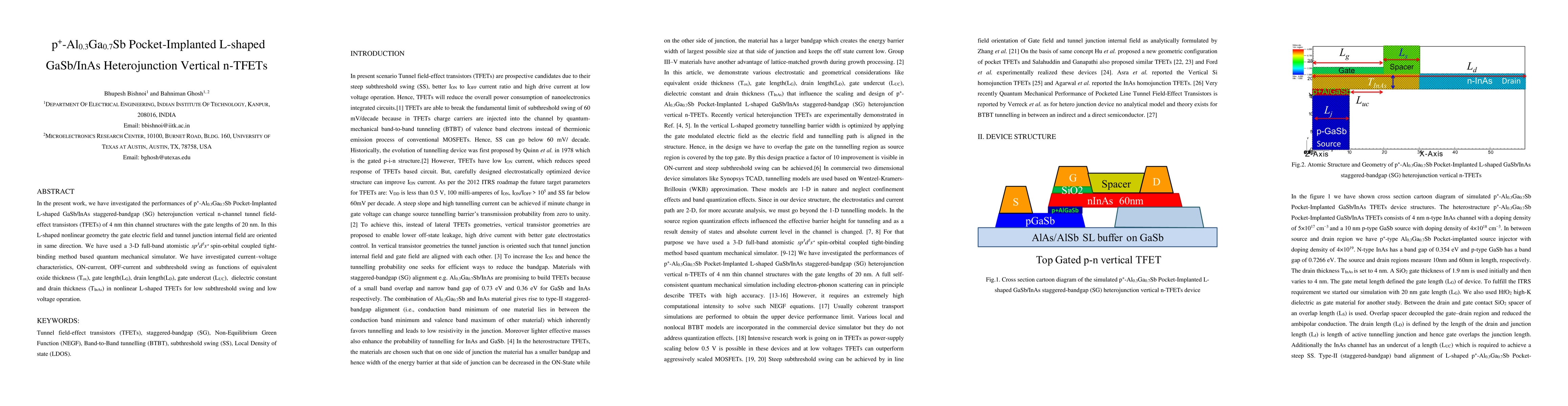
In the present work, we have investigated the performances of p plus minus Al0.3Ga0.7Sb Pocket Implanted L shaped GaSb InAs staggered bandgap SG heterojunction vertical n channel tunnel field effect transistors TFETs of 4 nm thin channel structures with the gate lengths of 20 nm. In this L shaped nonlinear geometry the gate electric field and tunnel junction internal field are oriented in same direction. We have used a 3 D full band atomistic sp3d5s spin orbital coupled tight binding method based quantum mechanical simulator. We have investigated current voltage characteristics, ON current, OFF current and subthreshold swing as functions of equivalent oxide thickness Tox, gate length LG, drain length LD, gate undercut LUC, dielectric constant and drain thickness TInAs in nonlinear L shaped TFETs for low subthreshold swing and low voltage operation.
AI Key Findings
Get AI-generated insights about this paper's methodology, results, significance, and more — seven facets brought into focus.
Impact
Paper Details
PDF Preview
Key Terms
Citation Network
Current paper (gray), citations (green), references (blue)
Display is limited for performance on very large graphs.
Discussion 0