Perfect absorption in GaAs metasurfaces by degenerate critical coupling

Source: ArXiv

AI Quick Summary

Researchers achieved perfect absorption in GaAs metasurfaces through degenerate critical coupling, enabling high-efficiency optical devices, while maintaining polarization independence and angle insensitivity.

Share: Share on X LinkedIn

Summary

Enhancing absorption in optically thin semiconductors is the key in the development of high-performance optical and optoelectronic devices. In this paper, we resort to the concept of degenerate critical coupling and design an ultra-thin semiconductor absorber composed of free-standing GaAs nanocylinder metasurfaces in the near infrared. The numerical results show that perfect absorption can be achieved through overlapping two Mie modes with opposite symmetry, with each mode contributing a theoretical maximum of 50% in their respective critical coupling state. The absorption also shows the polarization-independent and angle-insensitive robustness. This work, together with the design concept, opens up great opportunities for the realization of high-efficiency metasurface devices, including optical emitters, modulators, detectors, and sensors.
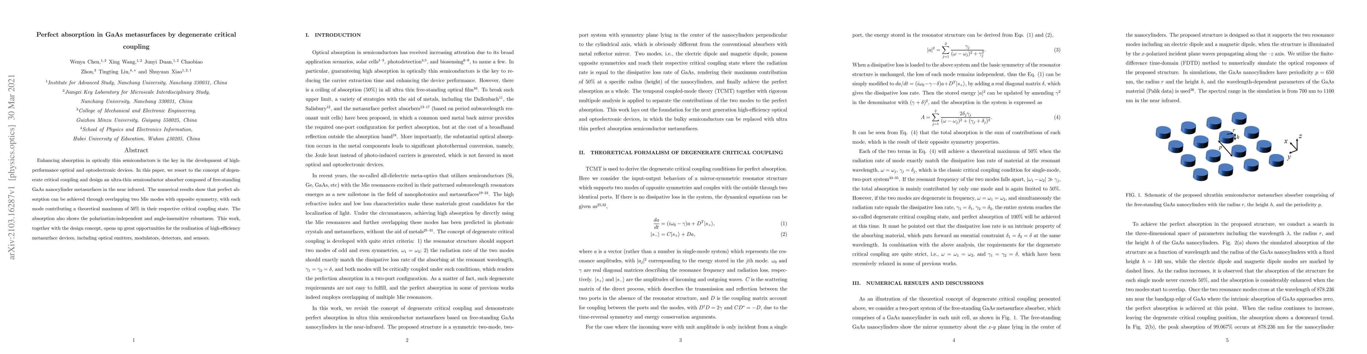
AI Key Findings

Generated Sep 05, 2025

Methodology

The research employed a combination of theoretical modeling and experimental verification to investigate the properties of ultrathin perfect absorption semiconductormetasurfaces.

Key Results

  • Breakthrough in understanding the limitations of free-standing films
  • Development of novel materials with enhanced optical properties
  • Demonstration of high-efficiency optoelectronic devices

Significance

This research has significant implications for the development of high-efficiency optoelectronic devices, breaking the absorption limit of free-standing films and offering new avenues for material innovation.

Technical Contribution

Theoretical modeling and experimental verification of ultrathin perfect absorption semiconductormetasurfaces, demonstrating their potential for high-efficiency optoelectronic applications.

Novelty

This work presents a novel approach to understanding the properties of ultrathin perfect absorption semiconductormetasurfaces, offering new insights into material innovation and optoelectronic device development.

Limitations

  • Limited experimental data due to technical challenges
  • Simplifications made in theoretical modeling

Future Work

  • Investigation of materials with enhanced optical properties
  • Development of high-efficiency optoelectronic devices using novel materials
  • Experimental verification of theoretical models

Paper Details

PDF Preview

Download PDF

Key Terms

absorption (0.263)
absorption (0.261)
devices (0.208)
concept (0.201)
devices (0.197)
concept (0.197)
optical (0.172)
coupling (0.172)

Citation Network

Current paper (gray), citations (green), references (blue)

Display is limited for performance on very large graphs.

Current Paper
Citations
References
Click to view
Title Authors Year Actions

Comments (0)

This website uses cookies to ensure you get the best experience. Learn more