Performance studies of the CE-65v2 MAPS prototype structure

Source: ArXiv

AI Quick Summary

This paper investigates the performance of the CE-65v2 MAPS prototype structure, focusing on its analogue charge collection properties in various pixel pitches and processes. Test beam data at CERN SPS revealed hit efficiencies of ≥99% and spatial resolutions better than 5 µm, with some variants achieving resolutions below 3 µm.

Share: Share on X LinkedIn

Summary

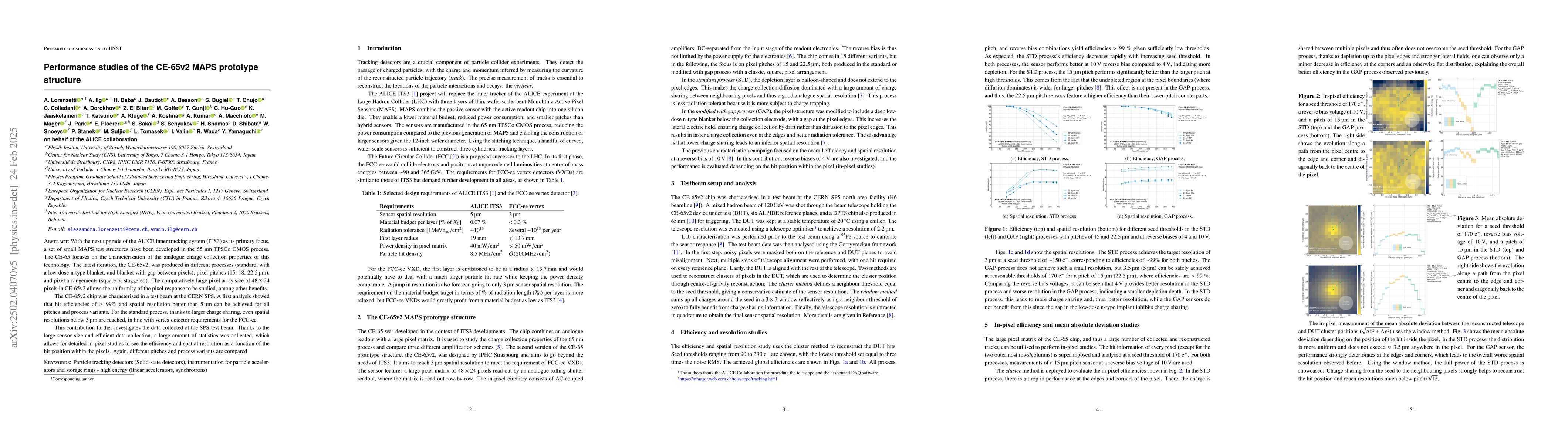
With the next upgrade of the ALICE inner tracking system (ITS3) as its primary focus, a set of small MAPS test structures have been developed in the 65 nm TPSCo CMOS process. The CE-65 focuses on the characterisation of the analogue charge collection properties of this technology. The latest iteration, the CE-65v2, was produced in different processes (standard, with a low-dose n-type blanket, and blanket with gap between pixels), pixel pitches (15, 18, 22.5 $\mu$m), and pixel arrangements (square or staggered). The comparatively large pixel array size of $48\times24$ pixels in CE-65v2 allows the uniformity of the pixel response to be studied, among other benefits. The CE-65v2 chip was characterised in a test beam at the CERN SPS. A first analysis showed that hit efficiencies of $\geq 99\%$ and spatial resolution better than 5 $\mu$m can be achieved for all pitches and process variants. For the standard process, thanks to larger charge sharing, even spatial resolutions below 3 $\mu$m are reached, in line with vertex detector requirements for the FCC-ee. This contribution further investigates the data collected at the SPS test beam. Thanks to the large sensor size and efficient data collection, a large amount of statistics was collected, which allows for detailed in-pixel studies to see the efficiency and spatial resolution as a function of the hit position within the pixels. Again, different pitches and process variants are compared.

AI Key Findings

Generated Jun 11, 2025

Methodology

The CE-65v2 MAPS prototype structures were characterized using a test beam at CERN SPS, analyzing hit efficiencies and spatial resolution for various pixel pitches and process variants.

Key Results

  • Hit efficiencies of ≥ 99% and spatial resolution better than 5 µm achieved for all pitches and process variants.
  • Standard process variant reached spatial resolutions below 3 µm, meeting vertex detector requirements for FCC-ee due to larger charge sharing.

Significance

This research is crucial for the development of the ALICE inner tracking system (ITS3) upgrade, providing insights into the analog charge collection properties of the 65 nm TPSCo CMOS technology.

Technical Contribution

Detailed characterization of CE-65v2 MAPS prototype structures in various process variants and pixel pitches, providing essential data for the ALICE ITS3 upgrade.

Novelty

The large sensor size and efficient data collection of CE-65v2 enable in-depth analysis of pixel response uniformity and performance, offering unique insights into the 65 nm TPSCo CMOS technology.

Limitations

  • The paper does not discuss limitations explicitly, but further studies could explore performance under varying radiation levels and temperatures.

Future Work

  • Detailed in-pixel studies to understand efficiency and spatial resolution as a function of hit position within pixels.
  • Investigate the technology's behavior under different radiation levels and temperature conditions.

Paper Details

PDF Preview

Download PDF

Citation Network

Current paper (gray), citations (green), references (blue)

Display is limited for performance on very large graphs.

Current Paper
Citations
References
Click to view

No citations found for this paper.

Comments (0)

This website uses cookies to ensure you get the best experience. Learn more