Summary

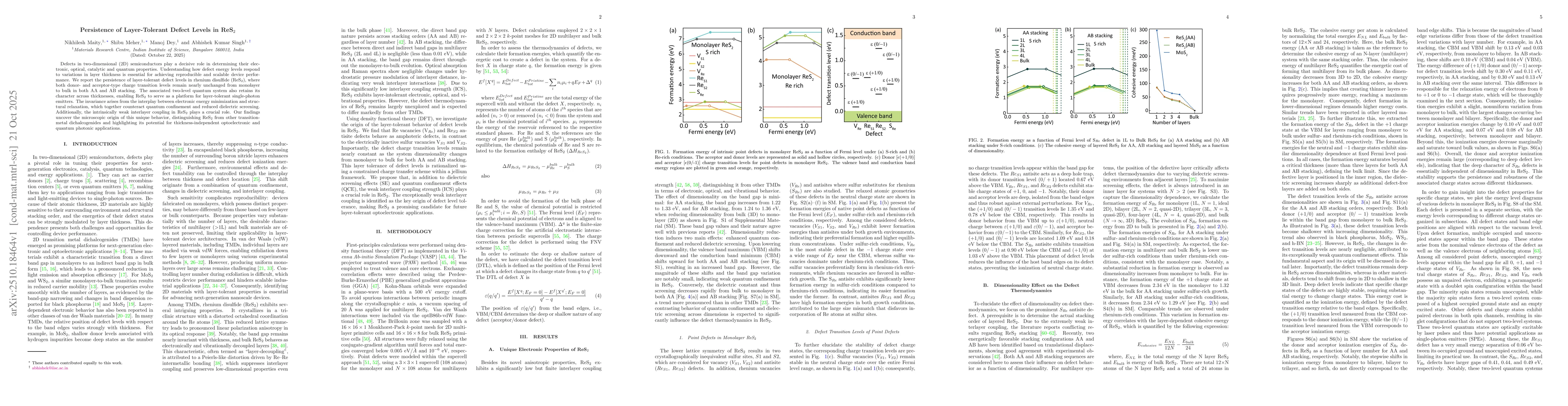
Defects in two-dimensional (2D) semiconductors play a decisive role in determining their electronic, optical, catalytic and quantum properties. Understanding how defect energy levels respond to variations in layer thickness is essential for achieving reproducible and scalable device performance. We report the persistence of layer-tolerant defect levels in rhenium disulfide (ReS2), where both donor- and acceptor-type charge transition levels remain nearly unchanged from monolayer to bulk in both AA and AB stacking. The associated two-level quantum system also retains its character across thicknesses, enabling ReS2 to serve as a platform for layer-tolerant single-photon emitters. The invariance arises from the interplay between electronic energy minimization and structural relaxation, which together counteract quantum confinement and reduced dielectric screening. Additionally, the intrinsically weak interlayer coupling in ReS2 plays a crucial role. Our findings uncover the microscopic origin of this unique behavior, distinguishing ReS2 from other transitionmetal dichalcogenides and highlighting its potential for thickness-independent optoelectronic and quantum photonic applications.

AI Key Findings

Generated Oct 24, 2025

Methodology

The study employed first-principles calculations using density functional theory (DFT) to investigate the electronic structure and defect properties of ReS2. The researchers analyzed the formation energies, charge transition levels, and optical properties of defects in different layer configurations.

Key Results

  • The electronic and optical properties of ReS2 are highly dependent on the stacking order and layer thickness.
  • Defect charge transition levels are significantly influenced by the dimensionality and layer stacking.
  • The monolayer form exhibits distinct electronic behavior compared to bulk ReS2 due to electronic and vibrational decoupling.

Significance

This research provides critical insights into the tunability of electronic and optical properties in ReS2, which is essential for developing next-generation optoelectronic devices and understanding defect behavior in 2D materials.

Technical Contribution

The work presents a comprehensive analysis of defect charge transition levels and their dependence on dimensionality and stacking order in ReS2, offering a framework for understanding defect behavior in layered materials.

Novelty

This study is novel in its systematic investigation of how stacking order and layer thickness influence defect properties in ReS2, providing a detailed understanding of the interplay between structural configuration and electronic behavior in 2D materials.

Limitations

  • The study is limited to computational simulations and does not include experimental validation.
  • The analysis focuses on specific defect types and may not cover all possible defect configurations.

Future Work

  • Experimental verification of the predicted defect properties and optical responses.
  • Investigation of other defect types and their impact on the electronic structure.
  • Exploration of hybrid systems combining ReS2 with other 2D materials for enhanced device performance.

Paper Details

PDF Preview

Download PDF

Comments (0)

This website uses cookies to ensure you get the best experience. Learn more