Photocurrents in a Single InAs Nanowire/ Silicon Heterojunction

Source: ArXiv

AI Quick Summary

This study investigates the optoelectronic properties of single InAs nanowires on p-doped silicon substrates, revealing photocurrent characteristics due to mid-gap trap states at the Si/InAs heterojunctions, which enable a photovoltaic effect at low bias and a photoconductance effect in the nanowires at higher biases.

Share: Share on X LinkedIn

Summary

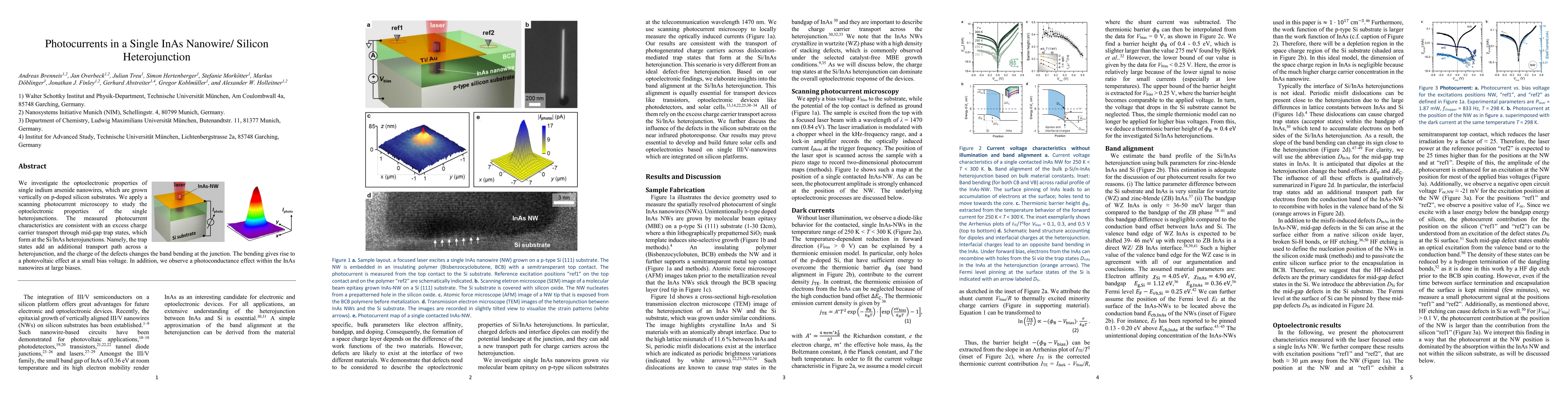
We investigate the optoelectronic properties of single indium arsenide nanowires, which are grown vertically on p-doped silicon substrates. We apply a scanning photocurrent microscopy to study the optoelectronic properties of the single heterojunctions. The measured photocurrent characteristics are consistent with an excess charge carrier transport through mid-gap trap states, which form at the Si/InAs heterojunctions. Namely, the trap states add an additional transport path across a heterojunction, and the charge of the defects changes the band bending at the junction. The bending gives rise to a photovoltaic effect at a small bias voltage. In addition, we observe a photoconductance effect within the InAs nanowires at large biases.

AI Key Findings

Generated Sep 03, 2025

Methodology

The study investigates optoelectronic properties of single InAs nanowires grown on p-doped silicon substrates using scanning photocurrent microscopy to analyze heterojunctions.

Key Results

  • Excess charge carrier transport through mid-gap trap states at Si/InAs heterojunctions.
  • Observation of a photovoltaic effect at small bias voltages due to trap state-induced band bending.
  • Detection of a photoconductance effect within InAs nanowires at large biases.

Significance

This research contributes to understanding the optoelectronic behavior of III/V nanowire-silicon heterojunctions, which is crucial for future photovoltaic and optoelectronic devices.

Technical Contribution

Detailed analysis of photocurrent characteristics in single InAs nanowire/silicon heterojunctions, attributing observed effects to mid-gap trap states.

Novelty

Provides comprehensive insights into the role of mid-gap defects in photocurrent dynamics across single Si/InAs heterojunctions, distinguishing between photovoltaic and photoconductance effects.

Limitations

  • Study is limited to single InAs nanowires on silicon substrates.
  • Results may not be directly generalizable to other semiconductor combinations or device architectures.

Future Work

  • Explore the behavior of other III/V nanowires on silicon platforms.
  • Investigate the impact of varying growth parameters on heterojunction properties.

Paper Details

PDF Preview

Download PDF

Key Terms

bending (0.316)
nanowires (0.300)
bending (0.296)
trap (0.279)
trap (0.275)
charge (0.221)
transport (0.213)
transport (0.202)
Title Authors Year Actions

Comments (0)

This website uses cookies to ensure you get the best experience. Learn more