Summary
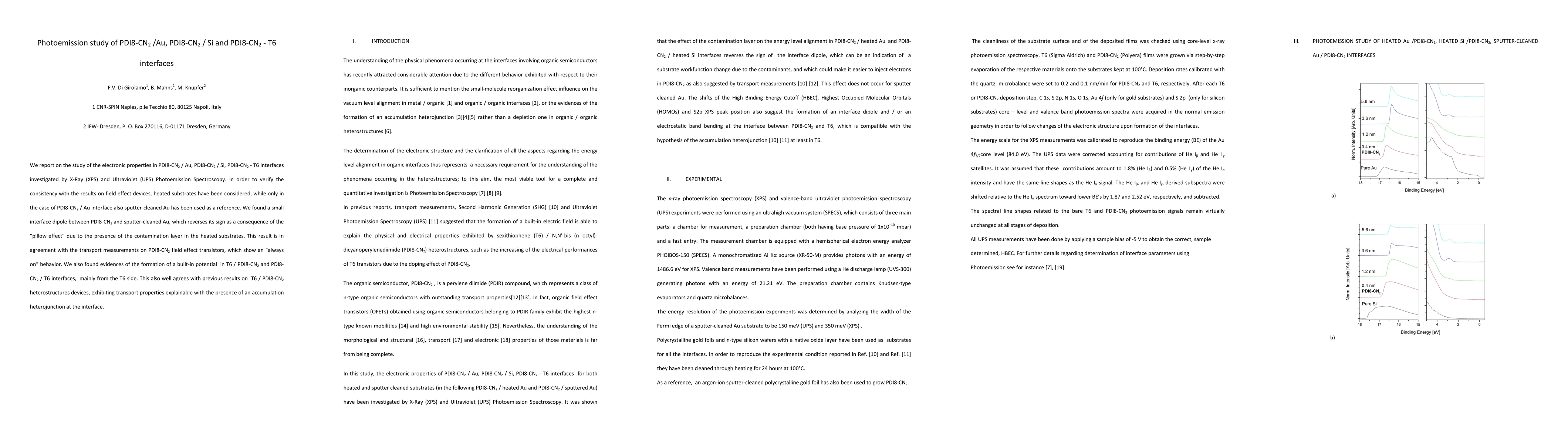
We report on the study of the electronic properties in PDI8-CN2 / Au, PDI8-CN2 / Si, PDI8-CN2 - T6 interfaces investigated by X-Ray (XPS) and Ultraviolet (UPS) Photoemission Spectroscopy. In order to verify the consistency with the results on field effect devices, heated substrates have been considered, while only in the case of PDI8-CN2 / Au interface also sputter-cleaned Au has been used as a reference. We found a small interface dipole between PDI8-CN2 and sputter-cleaned Au, which reverses its sign as a consequence of the 'pillow effect' due to the presence of the contamination layer in the heated substrates. This result is in agreement with the transport measurements on PDI8-CN2 field effect transistors, which show an 'always on' behavior. We also found evidences of the formation of a built-in potential in T6 / PDI8-CN2 and PDI8-CN2 / T6 interfaces, mainly from the T6 side. This also well agrees with previous results on T6 / PDI8-CN2 heterostructures devices, exhibiting transport properties explainable with the presence of an accumulation heterojunction at the interface.
AI Key Findings
Get AI-generated insights about this paper's methodology, results, and significance.
Paper Details
PDF Preview
Key Terms
Citation Network
Current paper (gray), citations (green), references (blue)
Display is limited for performance on very large graphs.
Similar Papers
Found 4 papers| Title | Authors | Year | Actions |
|---|
Comments (0)