The research presents a three-terminal superconducting switch (wTron) fabricated using photolithography, which can directly interface with CMOS electronics. The study investigates the switching characteristics by varying channel and gate dimensions and bias currents.
Photolithography-Compatible Three-Terminal Superconducting Switch for Driving CMOS Loads
Publication
Metrics
AI Quick Summary
Researchers developed a photolithography-compatible superconducting switch that can interface with CMOS devices, enabling the interface between cryo-electronics and CMOS electronics for next-generation computing applications.
Quick Answers
What is "Photolithography-Compatible Three-Terminal Superconducting Switch for Driving CMOS Loads" about?
Researchers developed a photolithography-compatible superconducting switch that can interface with CMOS devices, enabling the interface between cryo-electronics and CMOS electronics for next-generation computing applications.
What methodology did the authors use?
The research presents a three-terminal superconducting switch (wTron) fabricated using photolithography, which can directly interface with CMOS electronics. The study investigates the switching characteristics by varying channel and gate dimensions and bias currents. More in Methodology →
What are the key results?
wTron exhibits an output impedance exceeding 1 k$\Omega$ and reduced sensitivity to ambient magnetic noise. — wTrons have switching currents in the mA range, suitable for driving current-hungry and highly capacitive CMOS loads. More in Key Results →
Why is this work significant?
This research is significant as it facilitates the interface between superconducting electronics and CMOS, paving the way for the development of foundry-process-compatible cryo-electronics ecosystems for next-generation computing and quantum applications. More in Significance →
What are the main limitations?
The study did not explore the long-term stability and reliability of wTrons under varying thermal and magnetic conditions. — The performance of wTrons in complex hybrid cryo-electronic systems beyond simple CMOS loads was not demonstrated. More in Limitations →
Abstract
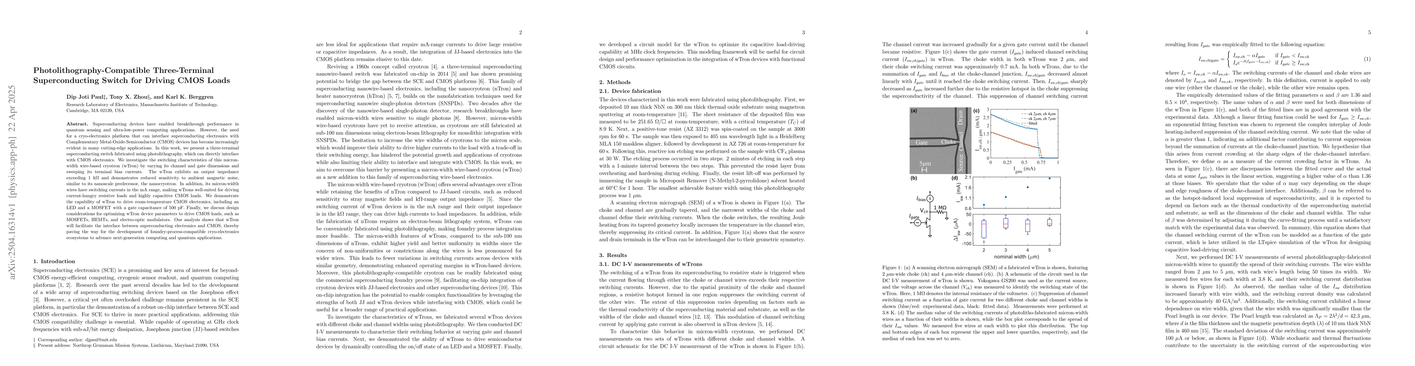
Superconducting devices have enabled breakthrough performance in quantum sensing and ultra-low-power computing applications. However, the need for a cryo-electronics platform that can interface superconducting electronics with Complementary Metal-Oxide-Semiconductor (CMOS) devices has become increasingly evident in many cutting-edge applications. In this work, we present a three-terminal superconducting switch fabricated using photolithography, which can directly interface with CMOS electronics. We investigate the switching characteristics of this micron-width wire-based cryotron (wTron) by varying its channel and gate dimensions and sweeping its terminal bias currents. The wTron exhibits an output impedance exceeding 1 k$\Omega$ and demonstrates reduced sensitivity to ambient magnetic noise, similar to its nanoscale predecessor, the nanocryotron. In addition, its micron-width wires have switching currents in the mA range, making wTrons well-suited for driving current-hungry resistive loads and highly capacitive CMOS loads. We demonstrate the capability of wTron to drive room-temperature CMOS electronics, including an LED and a MOSFET with a gate capacitance of 500 pF. Finally, we discuss design considerations for optimizing wTron device parameters to drive CMOS loads, such as MOSFETs, HEMTs, and electro-optic modulators. Our analysis shows that wTron will facilitate the interface between superconducting electronics and CMOS, thereby paving the way for the development of foundry-process-compatible cryo-electronics ecosystems to advance next-generation computing and quantum applications.
Key Findings, in focus
Seven facets of this paper, analysed and brought into focus by AI.
This research is significant as it facilitates the interface between superconducting electronics and CMOS, paving the way for the development of foundry-process-compatible cryo-electronics ecosystems for next-generation computing and quantum applications.
- wTron exhibits an output impedance exceeding 1 k$\Omega$ and reduced sensitivity to ambient magnetic noise.
- wTrons have switching currents in the mA range, suitable for driving current-hungry and highly capacitive CMOS loads.
- The wTron successfully demonstrated driving room-temperature CMOS electronics, including an LED and a MOSFET with a gate capacitance of 500 pF.
This research is significant as it facilitates the interface between superconducting electronics and CMOS, paving the way for the development of foundry-process-compatible cryo-electronics ecosystems for next-generation computing and quantum applications.
The paper introduces a photolithography-compatible micron-width wire-based cryotron (wTron) capable of directly interfacing with CMOS electronics, providing a promising solution for cryo-electronics platforms.
The wTron design offers a scalable and foundry-compatible alternative to nanoscale cryotrons, enabling the integration of superconducting and CMOS technologies for advanced computing and quantum applications.
- The study did not explore the long-term stability and reliability of wTrons under varying thermal and magnetic conditions.
- The performance of wTrons in complex hybrid cryo-electronic systems beyond simple CMOS loads was not demonstrated.
- Investigate the long-term stability and reliability of wTrons in diverse operating conditions.
- Explore the applicability and performance of wTrons in more complex hybrid cryo-electronic systems.
Impact
Paper Details
Authors
PDF Preview
Citation Network
Current paper (gray), citations (green), references (blue)
Display is limited for performance on very large graphs.
Discussion 0