Photoluminescent colour centres on a mainstream silicon photonic foundry platform

Source: ArXiv

AI Quick Summary

This paper demonstrates the fabrication of W-centre photoluminescence on a mainstream silicon photonics platform via a foundry-compatible back end-of-line (BEOL) treatment, achieving brightness comparable to custom processes. This approach enables the integration of efficient on-chip classical and quantum light sources directly onto silicon photonic circuits, facilitating large-scale photonic architectures.

Share: Share on X LinkedIn

Summary

The fabrication of silicon photonic components in commercial CMOS-compatible foundries has revolutionized the impact of silicon photonics on advancing communication, quantum computing and artificial intelligence, due to their benefits of mass production, high throughput, low cost, and high performance. The indirect bandgap of silicon introduces a fundamental challenge; thus, the mainstream silicon-on-insulator (SOI) platform does not have efficient light sources. Recently, luminescent colour centres in SOI have emerged as one promising approach for developing efficient on-chip classical and quantum light sources, although past work has relied on custom fabrication that is not foundry-compatible. In this work, we demonstrate W-centre photoluminescence on a mainstream silicon photonics platform through development of a straightforward back end-of-line (BEOL) treatment. At an optimal implant energy of 7~MeV, we observed W-centre photoluminescence with a brightness comparable to prior in-house processes. We performed a series of experiments on Circular Bragg Grating (CBG) devices with varying pitches, duty cycles, and implant energies to confirm the PL emission from the encapsulated SOI device layer rather than the handle wafer. Our novel approach in fabricating silicon colour centres in commercial silicon photonic foundry processes opens up new opportunities for integrating classical and quantum light sources directly onto silicon photonic circuits, unlocking opportunities for large-scale integration of advanced photonic architectures on chip.
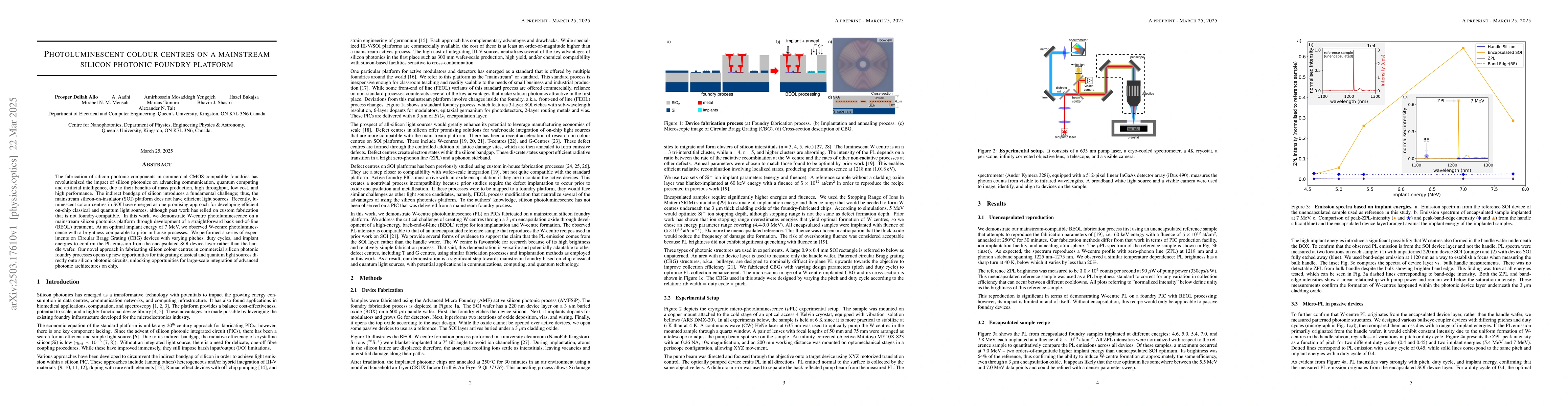
AI Key Findings

Generated Jun 10, 2025

Methodology

The research utilized a straightforward back-end-of-line (BEOL) treatment on a mainstream silicon photonic foundry platform, involving ion implantation and annealing processes to induce W-center photoluminescence in silicon-on-insulator (SOI) devices.

Key Results

  • Demonstrated W-centre photoluminescence with brightness comparable to prior in-house processes on a mainstream silicon photonic foundry platform.
  • Achieved maximum brightness at 7 MeV implant energy, approximately two orders of magnitude higher than unencapsulated SOI optimum, confirming efficient W-centre formation through a 3 µm cladding oxide.
  • Confirmed PL emission originated from the encapsulated SOI device layer rather than the handle wafer through experiments on Circular Bragg Grating (CBG) devices with varying pitches, duty cycles, and implant energies.

Significance

This work opens up new opportunities for integrating classical and quantum light sources directly onto silicon photonic circuits, unlocking possibilities for large-scale integration of advanced photonic architectures on-chip, which is crucial for communication, quantum computing, and artificial intelligence applications.

Technical Contribution

The paper presents a novel approach for creating luminescent color centers in commercial silicon photonic foundry processes, enabling the development of efficient on-chip classical and quantum light sources.

Novelty

This research distinguishes itself by successfully demonstrating W-centre photoluminescence on a mainstream silicon photonic foundry platform, unlike previous work that relied on custom fabrication not foundry-compatible.

Limitations

  • The study was limited to demonstrating W-centre PL on a foundry platform; further research is needed to explore the scalability and long-term stability of these color centers.
  • The research focused on specific implant energies and fluences; additional studies are required to optimize these parameters for various applications.

Future Work

  • Explore the potential of electrical pumping for fully integrated cryogenic photonic systems.
  • Investigate the integration of W-centres into microcavity designs for the development of efficient on-chip silicon lasers using foundry-fabricated emitters.

Paper Details

PDF Preview

Download PDF

Citation Network

Current paper (gray), citations (green), references (blue)

Display is limited for performance on very large graphs.

Current Paper
Citations
References
Click to view

No citations found for this paper.

Comments (0)

This website uses cookies to ensure you get the best experience. Learn more