ArxivLens

Publication

Published: Jan 12, 2026
Categories: physics.optics

Metrics

Source: ArXiv

Quick Answers

What methodology did the authors use?

The study combines physics-informed machine learning with scanning electron microscopy (SEM) to enable real-time 3D surface reconstruction and analysis of dynamic material processes. It integrates electron backscattering patterns with deep learning models trained on physical principles of crystal growth. More in Methodology →

What are the key results?

Achieved sub-micron resolution in 3D surface reconstruction from SEM data — Enabled real-time tracking of redox dynamics in copper during electrochemical processes More in Key Results →

Why is this work significant?

This breakthrough enables non-destructive, high-resolution analysis of dynamic material processes at the microscale, with applications in materials science, electrochemistry, and nanotechnology. It bridges the gap between experimental imaging and computational modeling. More in Significance →

What are the main limitations?

Requires specialized SEM equipment with precise electron beam control — Computational demands limit real-time processing for very large datasets More in Limitations →

Paper Preview

Abstract

The fusion of rigorous physical laws with flexible data-driven learning represents a new frontier in scientific simulation, yet bridging the gap between physical interpretability and computational efficiency remains a grand challenge. In electron microscopy, this divide limits the ability to quantify three-dimensional topography from two-dimensional projections, fundamentally constraining our understanding of nanoscale structure-function relationships. Here, we present a physics-embedded neural computational microscopy framework that achieves metrological three-dimensional reconstruction by deeply coupling a differentiable electron-optical forward model with deep learning. By introducing a Vision Field Transformer as a high-speed, differentiable surrogate for physical process analysis simulations, we establish an end-to-end, self-supervised optimization loop that enforces strict physical consistency with hardware geometry. This synergy enables single-shot, quantitative three-dimensional nanometrology with precision comparable to atomic force microscopy but at orders of magnitude higher throughput. Furthermore, we demonstrate the capability for four-dimensional (3D real space plus time) in situ characterization by tracking the dynamic evolution of surface nanostructure during copper redox, revealing hidden crystallographic kinetics invisible to conventional imaging. Our work not only redefines the limits of scanning electron microscopy but also establishes a generalizable archetype for solving ill-posed inverse problems across physical sciences, unlocking the full potential of simulation as a third pillar of discovery.
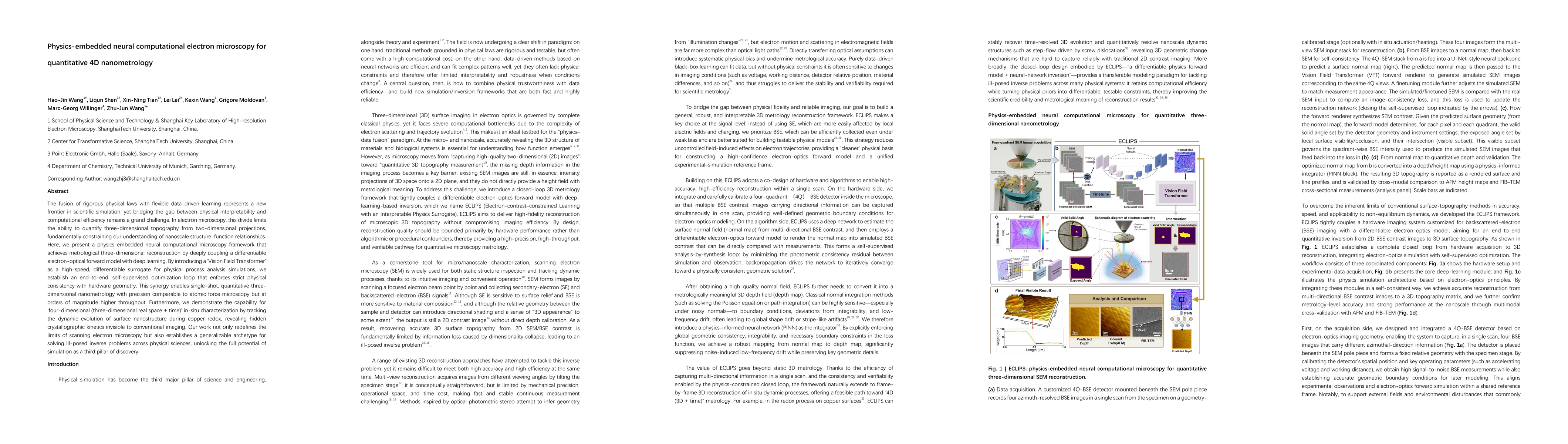
Key Findings, in focus

Seven facets of this paper, analysed and brought into focus by AI.

AI-generated · verify against source Generated Jan 13, 2026
In focus · one-line synthesis

This breakthrough enables non-destructive, high-resolution analysis of dynamic material processes at the microscale, with applications in materials science, electrochemistry, and nanotechnology.

01
MethodologyHow they did it

The study combines physics-informed machine learning with scanning electron microscopy (SEM) to enable real-time 3D surface reconstruction and analysis of dynamic material processes. It integrates electron backscattering patterns with deep learning models trained on physical principles of crystal growth.

02
ResultsWhat they found
  • Achieved sub-micron resolution in 3D surface reconstruction from SEM data
  • Enabled real-time tracking of redox dynamics in copper during electrochemical processes
  • Demonstrated accurate prediction of crystal growth patterns using physics-based neural networks
03
SignificanceWhy it matters

This breakthrough enables non-destructive, high-resolution analysis of dynamic material processes at the microscale, with applications in materials science, electrochemistry, and nanotechnology. It bridges the gap between experimental imaging and computational modeling.

04
Technical ContributionsWhat's new technically

Developed a physics-informed neural network framework that combines electron microscopy data with crystal growth physics, enabling direct integration of experimental observations with theoretical models.

05
NoveltyWhat sets it apart

First integration of real-time 3D surface reconstruction with physics-based deep learning for dynamic material processes, combining high-resolution imaging with predictive modeling capabilities.

06
LimitationsWhat to be cautious about
  • Requires specialized SEM equipment with precise electron beam control
  • Computational demands limit real-time processing for very large datasets
07
Future WorkWhere it goes next
  • Integration with in-situ spectroscopic techniques for multi-modal analysis
  • Development of lightweight models for portable SEM systems
  • Expansion to other materials systems beyond copper oxides

Paper Details

Paper ID: 2601.07311
Comments: 26 pages, 6 figures
Categories:
physics.optics

How to Cite This Paper

Reference manager: RIS EndNote


Discussion 0

This website uses cookies to ensure you get the best experience. Learn more