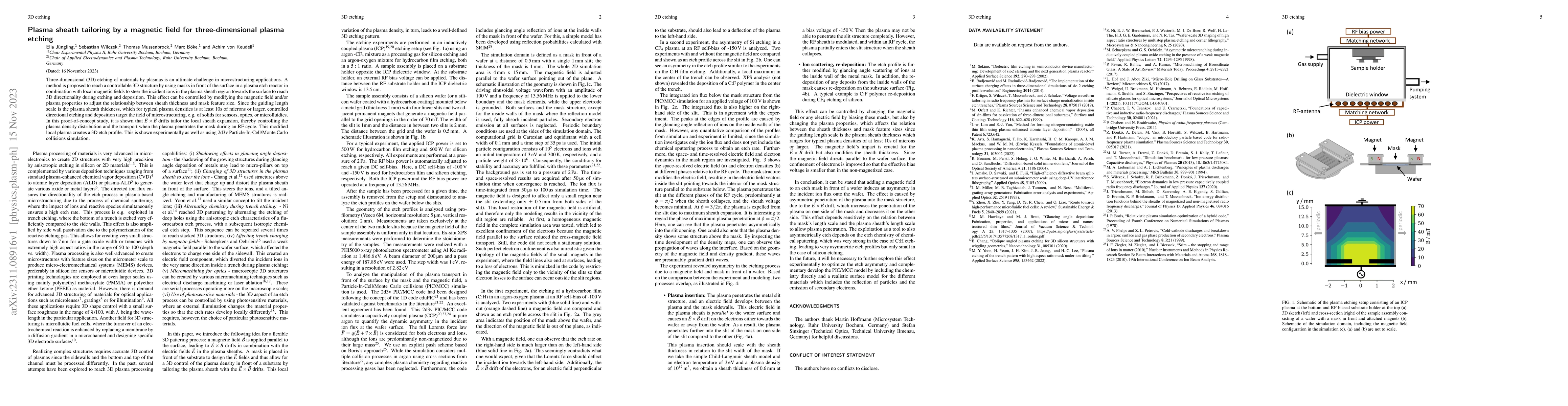
Plasma sheath tailoring by a magnetic field for three-dimensional plasma etching
Publication
Metrics
AI Quick Summary
This paper proposes a method to achieve controllable three-dimensional plasma etching by using masks and local magnetic fields to steer ions in the plasma sheath region, thereby enabling precise microstructuring. Experimental and simulation results demonstrate that $\vec{E}\times\vec{B}$ drifts can tailor the sheath expansion, leading to a 3D etch profile.
Paper Preview
Abstract
Three-dimensional (3D) etching of materials by plasmas is an ultimate challenge in microstructuring applications. A method is proposed to reach a controllable 3D structure by using masks in front of the surface in a plasma etch reactor in combination with local magnetic fields to steer the incident ions in the plasma sheath region towards the surface to reach 3D directionality during etching and deposition. This effect can be controlled by modifying the magnetic field and/or plasma properties to adjust the relationship between sheath thickness and mask feature size. Since the guiding length scale is the plasma sheath thickness, which for typical plasma densities is at least 10s of microns or larger, controlled directional etching and deposition target the field of microstructuring, e.g. of solids for sensors, optics, or microfluidics. In this proof-of-concept study, it is shown that $\vec{E}\times\vec{B}$ drifts tailor the local sheath expansion, thereby controlling the plasma density distribution and the transport when the plasma penetrates the mask during an RF cycle. This modified local plasma creates a 3D etch profile. This is shown experimentally as well as using 2d3v Particle-In-Cell/Monte Carlo collisions simulation.
AI Key Findings
Get AI-generated insights about this paper's methodology, results, significance, and more — seven facets brought into focus.
Impact
Paper Details
Authors
PDF Preview
Key Terms
Citation Network
Current paper (gray), citations (green), references (blue)
Display is limited for performance on very large graphs.
Discussion 0