Publication
Metrics
AI Quick Summary
This paper investigates the decay of surface plasmons to hot carriers at atomically sharp metal-semiconductor nanojunctions, using a monolithic Al-Ge heterostructure device. The study demonstrates electrostatic control over hot electron transfer, achieving momentum matching and negative differential resistance through interband electron transfer in Ge.
Paper Preview
Abstract
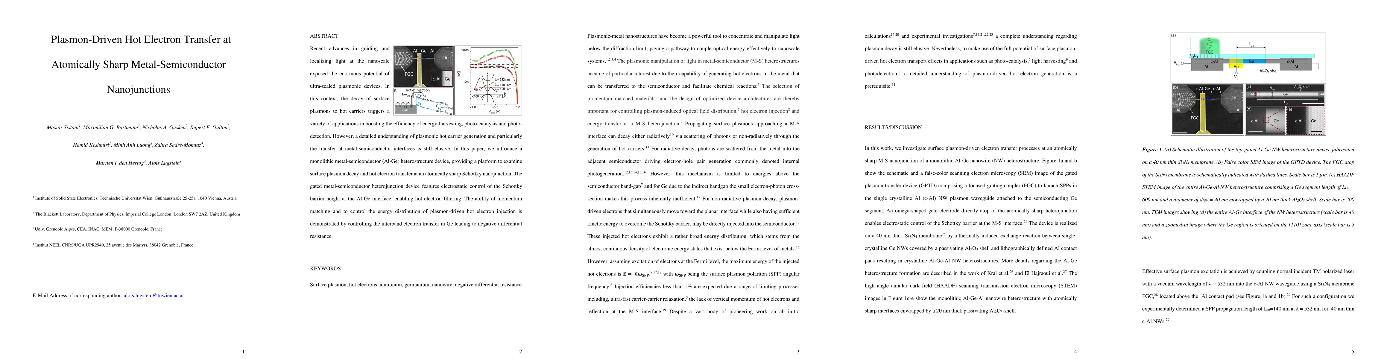
Recent advances in guiding and localizing light at the nanoscale exposed the enormous potential of ultra-scaled plasmonic devices. In this context, the decay of surface plasmons to hot carriers triggers a variety of applications in boosting the efficiency of energy-harvesting, photo-catalysis and photo-detection. However, a detailed understanding of plasmonic hot carrier generation and particularly the transfer at metal-semiconductor interfaces is still elusive. In this paper, we introduce a monolithic metal-semiconductor (Al-Ge) heterostructure device, providing a platform to examine surface plasmon decay and hot electron transfer at an atomically sharp Schottky nanojunction. The gated metal-semiconductor heterojunction device features electrostatic control of the Schottky barrier height at the Al-Ge interface, enabling hot electron filtering. The ability of momentum matching and to control the energy distribution of plasmon-driven hot electron injection is demonstrated by controlling the interband electron transfer in Ge leading to negative differential resistance.
AI Key Findings
Get AI-generated insights about this paper's methodology, results, significance, and more — seven facets brought into focus.
Impact
Paper Details
Authors
PDF Preview
Key Terms
Citation Network
Current paper (gray), citations (green), references (blue)
Display is limited for performance on very large graphs.
Discussion 0