Plasmonic Optical Modulator based on Adiabatic Coupled Waveguides
Publication
Metrics
AI Quick Summary
This paper proposes a plasmonic optical modulator based on adiabatically coupled waveguides, achieving high modulation depth and low insertion loss by electrostatically tuning the free-carrier concentration in a central waveguide. The design demonstrates an energy efficiency of 40 atto-joules per bit and a high extinction ratio, promising for next-generation optical interconnects.
Paper Preview
Abstract
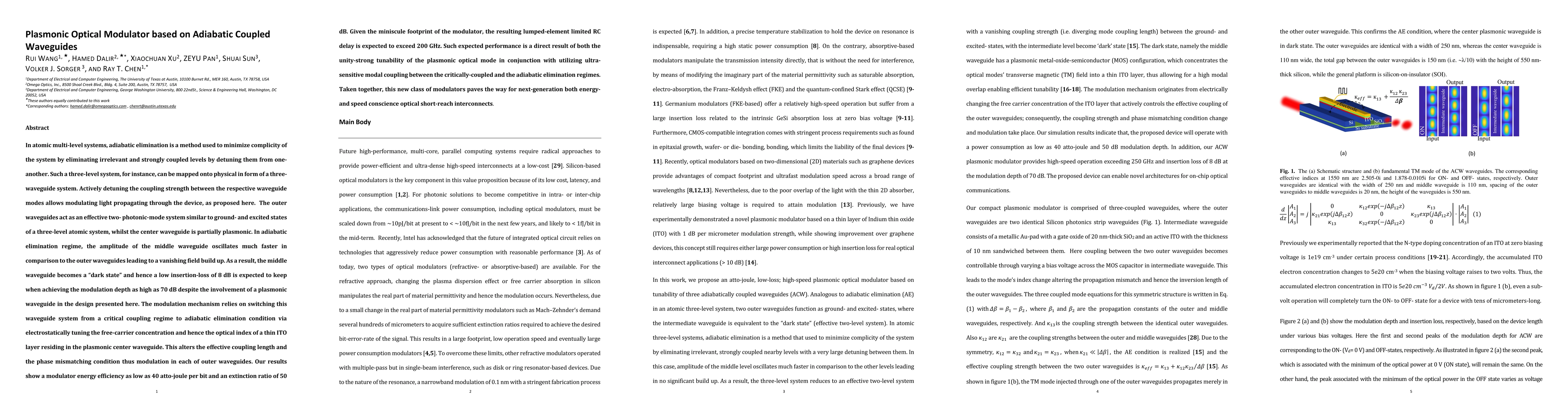
In atomic multi-level systems, adiabatic elimination is a method used to minimize complicity of the system by eliminating irrelevant and strongly coupled levels by detuning them from one-another. Such a three-level system, for instance, can be mapped onto physical in form of a three-waveguide system. Actively detuning the coupling strength between the respective waveguide modes allows modulating light propagating through the device, as proposed here. The outer waveguides act as an effective two- photonic-mode system similar to ground- and excited states of a three-level atomic system, whilst the center waveguide is partially plasmonic. In adiabatic elimination regime, the amplitude of the middle waveguide oscillates much faster in comparison to the outer waveguides leading to a vanishing field build up. As a result, the middle waveguide becomes a dark state and hence a low insertion-loss of 8 decibel is expected to keep when achieving the modulation depth as high as 70 decibel despite the involvement of a plasmonic waveguide in the design presented here. The modulation mechanism relies on switching this waveguide system from a critical coupling regime to adiabatic elimination condition via electrostatically tuning the free-carrier concentration and hence the optical index of a thin ITO layer residing in the plasmonic center waveguide. This alters the effective coupling length and the phase mismatching condition thus modulation in each of outer waveguides. Our results show a modulator energy efficiency as low as 40 atto-joule per bit and an extinction ratio of 50 decibel. Given the minuscule footprint of the modulator, the resulting lumped-element limited RC delay is expected to exceed 200 giga hertz. This type of modulator paves the way for next-generation both energy-and speed conscience optical short-reach interconnects.
AI Key Findings
Get AI-generated insights about this paper's methodology, results, significance, and more — seven facets brought into focus.
Impact
Paper Details
PDF Preview
Key Terms
Citation Network
Current paper (gray), citations (green), references (blue)
Display is limited for performance on very large graphs.
Discussion 0