Publication
Metrics
AI Quick Summary
This paper introduces a method for creating small point contacts on encapsulated graphene using pre-patterned hexagonal boron nitride, achieving low contact resistances and demonstrating insulating behavior in the quantum Hall regime. The technique supports high mobility graphene structures and facilitates advanced electron optical applications.
Paper Preview
Abstract
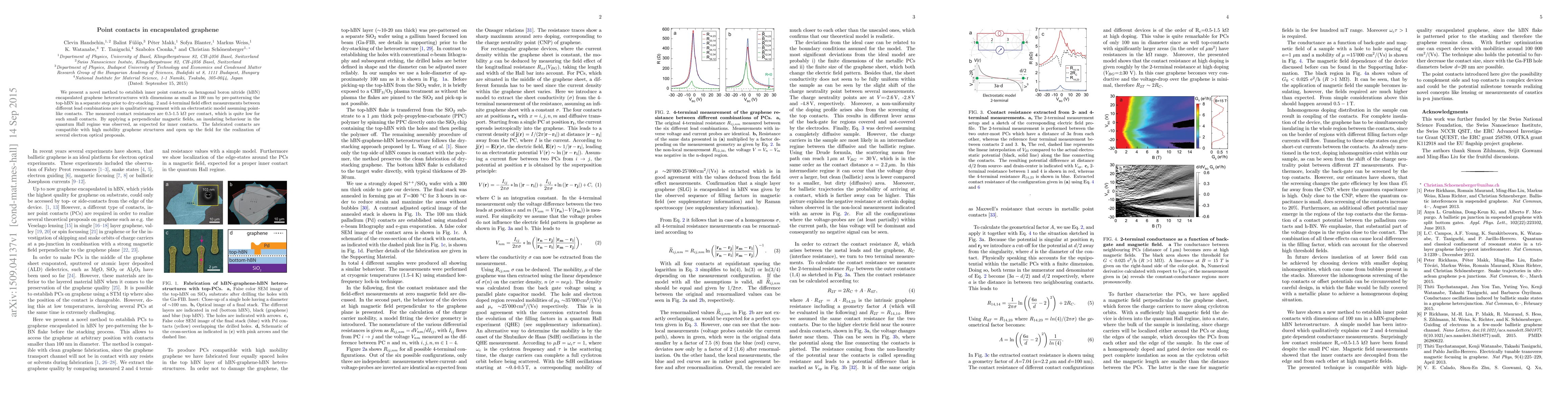
We present a novel method to establish inner point contacts on hexagonal boron nitride (hBN) encapsulated graphene heterostructures with dimensions as small as 100 nm by pre-patterning the top-hBN in a separate step prior to dry-stacking. 2 and 4-terminal field effect measurements between different lead combinations are in qualitative agreement with an electrostatic model assuming pointlike contacts. The measured contact resistances are 0.5-1.5 k$\Omega$ per contact, which is quite low for such small contacts. By applying a perpendicular magnetic fields, an insulating behaviour in the quantum Hall regime was observed, as expected for inner contacts. The fabricated contacts are compatible with high mobility graphene structures and open up the field for the realization of several electron optical proposals.
AI Key Findings
Get AI-generated insights about this paper's methodology, results, significance, and more — seven facets brought into focus.
Impact
Paper Details
PDF Preview
Key Terms
Citation Network
Current paper (gray), citations (green), references (blue)
Display is limited for performance on very large graphs.
Discussion 0