Polarization fields in GaN/AlN nanowire heterostructures studied by Off axis holography
Publication
Metrics
AI Quick Summary
This research uses off-axis holography to study the polarization fields in GaN/AlN nanowire heterostructures. Combining experimental results with theoretical calculations, it reveals insights into the potential distribution within these nanostructures, discussing the impact of surface states.
Paper Preview
Abstract
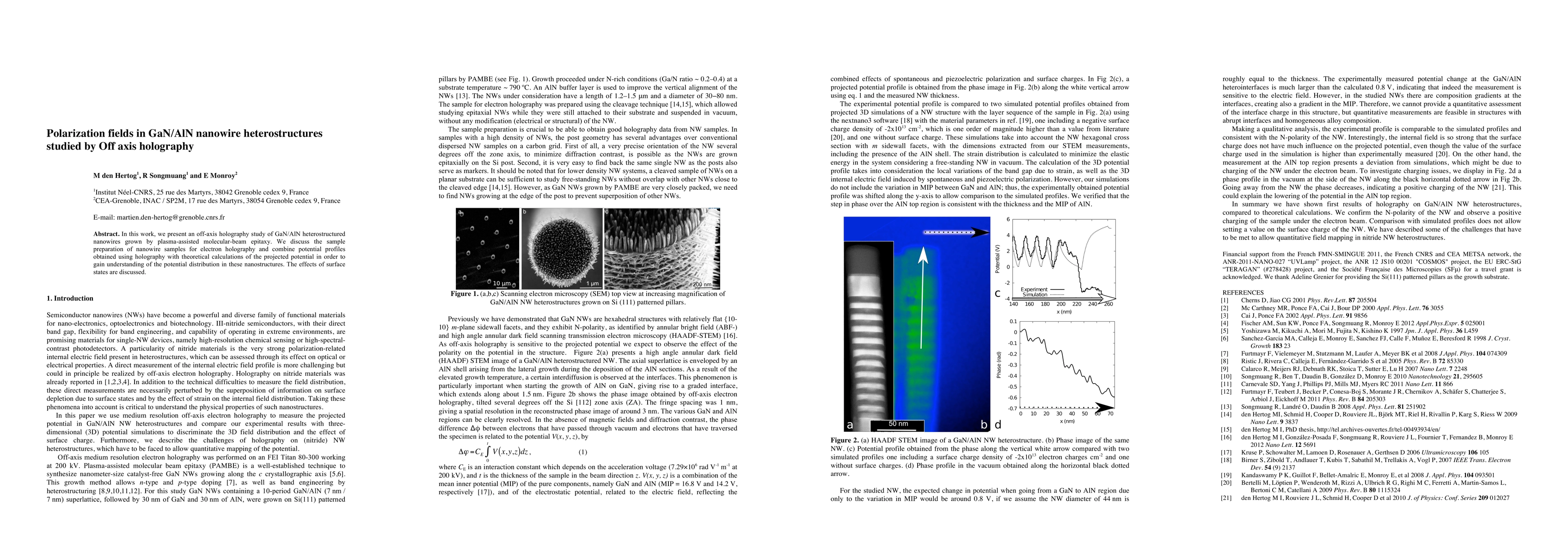
In this work, we present an off-axis holography study of GaN/AlN heterostructured nanowires grown by plasma-assisted molecular-beam epitaxy. We discuss the sample preparation of nanowire samples for electron holography and combine potential profiles obtained using holography with theoretical calculations of the projected potential in order to gain understanding of the potential distribution in these nanostructures. The effects of surface states are discussed
AI Key Findings
Get AI-generated insights about this paper's methodology, results, significance, and more — seven facets brought into focus.
Impact
Paper Details
PDF Preview
Key Terms
Citation Network
Current paper (gray), citations (green), references (blue)
Display is limited for performance on very large graphs.
Discussion 0