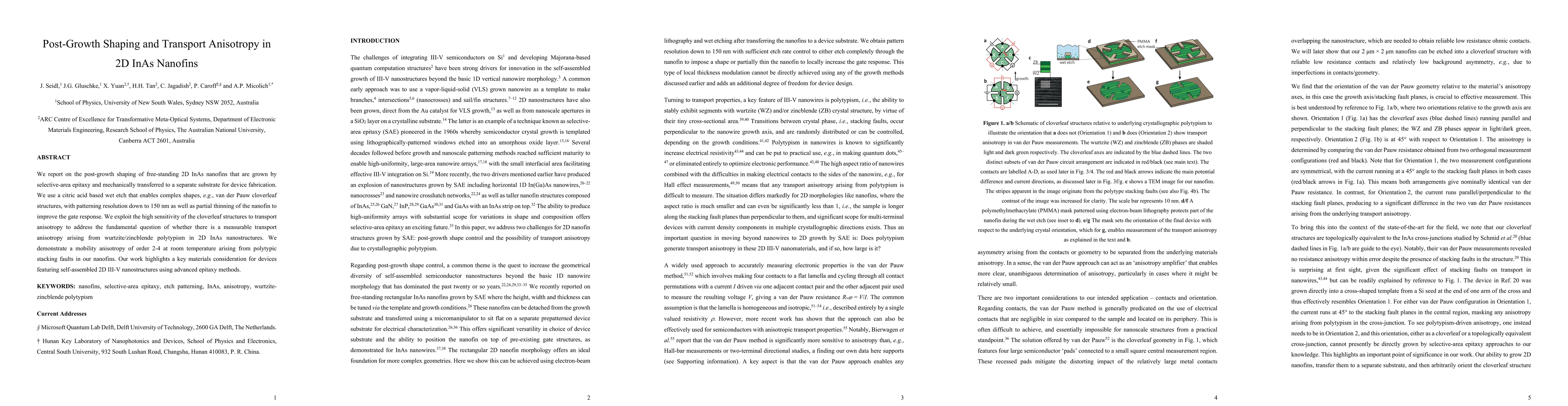
Impact of invasive metal probes on Hall measurements in semiconductor nanostructures.
|
J. G. Gluschke, J. Seidl, H. Tan, C. Jagadish, P. Caroff, A. Micolich
|
2020
|
View Paper
|
Exploring the Size Limitations of Wurtzite III-V Film Growth.
|
P. Staudinger, K. Moselund, H. Schmid
|
2019
|
View Paper
|
GaAs nanoscale membranes: prospects for seamless integration of III-Vs on silicon.
|
A. M. Raya, M. Friedl, Sara Martí-Sánchez, V. Dubrovskii, L. Francaviglia, B. Alén, N. Morgan, G. Tütüncüoglu, Q. Ramasse, D. Fuster, J. Llorens, J. Arbiol, A. Fontcuberta i Morral
|
2019
|
View Paper
|
Regaining a Spatial Dimension: Mechanically Transferrable Two-Dimensional InAs Nanofins Grown by Selective Area Epitaxy.
|
J. Seidl, J. G. Gluschke, Xiaoming Yuan, Xiaoming Yuan, S. Naureen, N. Shahid, H. Tan, C. Jagadish, A. Micolich, P. Caroff, P. Caroff
|
2019
|
View Paper
|
Shape Engineering of InP Nanostructures by Selective Area Epitaxy.
|
Naiyin Wang, Xiaoming Yuan, Xu Zhang, Q. Gao, Bijun Zhao, Li Li, M. Lockrey, H. Tan, C. Jagadish, P. Caroff
|
2019
|
View Paper
|
Vapor Phase Growth of Semiconductor Nanowires: Key Developments and Open Questions.
|
Lucas Güniat, P. Caroff, A. Fontcuberta i Morral
|
2019
|
View Paper
|
Nanosails Showcasing Zn3As2 as an Optoelectronic‐Grade Earth Abundant Semiconductor
|
E. Stutz, M. Friedl, T. Burgess, H. Tan, P. Caroff, C. Jagadish, A. Fontcuberta i Morral
|
2019
|
View Paper
|
Bottom‐Up Grown 2D InSb Nanostructures
|
S. Gazibegović, G. Badawy, Thijs L J Buckers, P. Leubner, Jie Shen, F. D. de Vries, S. Koelling, L. Kouwenhoven, M. Verheijen, E. Bakkers
|
2019
|
View Paper
|
Individually addressable double quantum dots formed with nanowire polytypes and identified by epitaxial markers
|
D. Barker, S. Lehmann, Luna Namazi, M. Nilsson, C. Thelander, K. Dick, V. Maisi
|
2019
|
View Paper
|
Two-Dimensional Quantum Transport in Free-Standing InSb Nanosheets.
|
N. Kang, Dingxun Fan, Jinhua Zhi, D. Pan, Sen Li, Cheng Wang, Jing-kun Guo, Jianhua Zhao, Hongqi Xu
|
2018
|
View Paper
|
Selectivity Map for Molecular Beam Epitaxy of Advanced III–V Quantum Nanowire Networks
|
P. Aseev, A. Fursina, F. Boekhout, Filip Krizek, Joachim E. Sestoft, F. Borsoi, S. Heedt, Guanzhong Wang, L. Binci, Sara Martí-Sánchez, T. Swoboda, R. Koops, E. Uccelli, J. Arbiol, P. Krogstrup, L. Kouwenhoven, Philippe Caroff
|
2018
|
View Paper
|
Dimension Engineering of High-Quality InAs Nanostructures on a Wafer Scale.
|
D. Pan, Ji-Yin Wang, Wei Zhang, Lujun Zhu, Xiaojun Su, Furong Fan, Yuhao Fu, Shaoyun Huang, D. Wei, Lijun Zhang, Manling Sui, A. Yartsev, Hongqi Xu, Jianhua Zhao
|
2018
|
View Paper
|
Achieving short high-quality gate-all-around structures for horizontal nanowire field-effect transistors
|
J. G. Gluschke, J. Seidl, Adam Burke, R. Lyttleton, D. Carrad, A. R. Ullah, S. Fahlvik, S. Lehmann, Heiner Linke, A. Micolich
|
2018
|
View Paper
|
Selective-area chemical beam epitaxy of in-plane InAs one-dimensional channels grown on InP(001), InP(111)B, and InP(011) surfaces
|
Joon Sue Lee, Sukgeun Choi, M. Pendharkar, D. Pennachio, B. Markman, M. Seas, S. Koelling, M. Verheijen, L. Casparis, K. Petersson, I. Petkovic, Vanessa Schaller, M. Rodwell, C. Marcus, P. Krogstrup, L. Kouwenhoven, E. Bakkers, C. Palmstrøm
|
2018
|
View Paper
|
Template-Assisted Scalable Nanowire Networks.
|
M. Friedl, Kris Cerveny, P. Weigele, G. Tütüncüoglu, Sara Martí-Sánchez, Chunyi Huang, T. Patlatiuk, H. Potts, Zhiyuan Sun, M. Hill, Lucas Güniat, Wonjong Kim, M. Zamani, V. Dubrovskii, J. Arbiol, L. Lauhon, D. Zumbühl, A. Fontcuberta i Morral
|
2018
|
View Paper
|
Field effect enhancement in buffered quantum nanowire networks
|
Filip Krizek, Joachim E. Sestoft, P. Aseev, Sara Martí-Sánchez, S. Vaitiekėnas, L. Casparis, S. Khan, Yu Liu, T. Stankevič, A. Whiticar, A. Fursina, F. Boekhout, R. Koops, E. Uccelli, L. Kouwenhoven, C. Marcus, J. Arbiol, P. Krogstrup
|
2018
|
View Paper
|
Majorana zero modes in superconductor–semiconductor heterostructures
|
R. Lutchyn, E. Bakkers, E. Bakkers, L. Kouwenhoven, P. Krogstrup, C. Marcus, Y. Oreg
|
2017
|
View Paper
|
Revealing Large-Scale Homogeneity and Trace Impurity Sensitivity of GaAs Nanoscale Membranes.
|
Zhuo Yang, A. Surrente, G. Tütüncüoglu, K. Gal̷kowski, M. Cazaban-Carrazé, F. Amaduzzi, P. Leroux, D. Maude, A. F. Morral, P. Płochocka
|
2017
|
View Paper
|
Ballistic One-Dimensional InAs Nanowire Cross-Junction Interconnects.
|
J. Gooth, M. Borg, H. Schmid, Vanessa Schaller, S. Wirths, K. Moselund, M. Luisier, S. Karg, H. Riel
|
2017
|
View Paper
|
Conduction Band Offset and Polarization Effects in InAs Nanowire Polytype Junctions.
|
I. Chen, S. Lehmann, M. Nilsson, Pyry Kivisaari, H. Linke, K. Dick, C. Thelander
|
2017
|
View Paper
|
InP Nanoflag Growth from a Nanowire Template by in Situ Catalyst Manipulation.
|
A. Kelrich, Ofir Sorias, Y. Calahorra, Y. Kauffmann, R. Gladstone, S. Cohen, M. Orenstein, D. Ritter
|
2016
|
View Paper
|
Twin-Induced InSb Nanosails: A Convenient High Mobility Quantum System.
|
M. de la Mata, R. Leturcq, S. Plissard, C. Rolland, C. Magén, J. Arbiol, P. Caroff
|
2016
|
View Paper
|
Single-electron transport in InAs nanowire quantum dots formed by crystal phase engineering
|
M. Nilsson, Luna Namazi, S. Lehmann, M. Leijnse, K. Dick, C. Thelander
|
2015
|
View Paper
|
Free-Standing Two-Dimensional Single-Crystalline InSb Nanosheets.
|
D. Pan, Dingxun Fan, Ning Kang, Jinhua Zhi, Xuezhe Yu, Hongqi Xu, Jianhua Zhao
|
2015
|
View Paper
|
Towards defect-free 1-D GaAs/AlGaAs heterostructures based on GaAs nanomembranes.
|
G. Tütüncüoglu, M. Mata, Davide Deiana, H. Potts, F. Matteini, Jordi Arbiol, A. F. Morral
|
2015
|
View Paper
|
Resolving ambiguities in nanowire field-effect transistor characterization.
|
S. Heedt, Isabel Otto, K. Sladek, H. Hardtdegen, J. Schubert, N. Demarina, H. Lüth, D. Grützmacher, T. Schäpers
|
2015
|
View Paper
|
Template-assisted selective epitaxy of III–V nanoscale devices for co-planar heterogeneous integration with Si
|
H. Schmid, M. Borg, K. Moselund, L. Gignac, C. Breslin, J. Bruley, D. Cutaia, H. Riel
|
2015
|
View Paper
|
III–V compound semiconductor transistors—from planar to nanowire structures
|
H. Riel, L. Wernersson, M. Hong, J. Alamo
|
2014
|
View Paper
|
Rationally Designed Single‐Crystalline Nanowire Networks
|
D. Car, J. Wang, M. Verheijen, E. Bakkers, S. Plissard
|
2014
|
View Paper
|
Nanometer-Scale Vertical-Sidewall Reactive Ion Etching of InGaAs for 3-D III-V MOSFETs
|
Xin Zhao, J. D. del Alamo
|
2014
|
View Paper
|
Formation and electronic properties of InSb nanocrosses.
|
S. Plissard, I. van Weperen, D. Car, M. Verheijen, G. Immink, J. Kammhuber, L. Cornelissen, D. Szombati, A. Geresdi, S. Frolov, L. Kouwenhoven, E. Bakkers
|
2013
|
View Paper
|
Electronic comparison of InAs wurtzite and zincblende phases using nanowire transistors
|
A. R. Ullah, H. Joyce, A. Burke, J. Wong-Leung, H. Tan, C. Jagadish, A. Micolich
|
2013
|
View Paper
|
Vertical "III-V" V-shaped nanomembranes epitaxially grown on a patterned Si[001] substrate and their enhanced light scattering.
|
S. Conesa‐Boj, E. Russo-Averchi, A. Dalmau-Mallorquí, J. Trevino, E. Pecora, C. Forestiere, Alex Handin, M. Ek, Ludovit P. Zweifel, L. Wallenberg, D. Rüffer, M. Heiss, D. Troadec, L. Dal Negro, P. Caroff, A. Fontcuberta i Morral
|
2012
|
View Paper
|
Dislocation reduction of InAs nanofins prepared on Si substrate using metal-organic vapor-phase epitaxy
|
Chao-Wei Hsu, Yung-Feng Chen, Y. Su
|
2012
|
View Paper
|
Spatially resolved Hall effect measurement in a single semiconductor nanowire.
|
K. Storm, Filip Halvardsson, M. Heurlin, D. Lindgren, A. Gustafsson, Phillip M. Wu, B. Monemar, L. Samuelson
|
2012
|
View Paper
|
Hall effect measurements on InAs nanowires
|
C. Blömers, T. Grap, M. Lepsa, J. Moers, S. Trellenkamp, D. Grützmacher, H. Lüth, T. Schäpers
|
2012
|
View Paper
|
A III–V nanowire channel on silicon for high-performance vertical transistors
|
K. Tomioka, M. Yoshimura, T. Fukui
|
2012
|
View Paper
|
Vertical nonpolar growth templates for light emitting diodes formed with GaN nanosheets
|
T. Yeh, Yen‐Ting Lin, B. Ahn, L. Stewart, P. Dapkus, S. Nutt
|
2012
|
View Paper
|
Effects of crystal phase mixing on the electrical properties of InAs nanowires.
|
C. Thelander, P. Caroff, S. Plissard, A. Dey, K. Dick
|
2011
|
View Paper
|
Anisotropic transport properties in InAs/AlSb heterostructures
|
G. Moschetti, Huan Zhao, P. Nilsson, Shumin Wang, A. Kalabukhov, G. Dambrine, S. Bollaert, L. Desplanque, X. Wallart, J. Grahn
|
2010
|
View Paper
|
Crystal phase quantum dots.
|
N. Akopian, G. Patriarche, L. Liu, J. Harmand, V. Zwiller
|
2010
|
View Paper
|
Correlating the nanostructure and electronic properties of InAs nanowires.
|
M. D. Schroer, J. Petta
|
2009
|
View Paper
|
Predicted band structures of III-V semiconductors in the wurtzite phase
|
A. De, C. Pryor
|
2009
|
View Paper
|
Structural and Room‐Temperature Transport Properties of Zinc Blende and Wurtzite InAs Nanowires
|
S. Dayeh, D. Susac, K. Kavanagh, E. Yu, Deli Wang
|
2009
|
View Paper
|
Twinning superlattices in indium phosphide nanowires
|
R. Algra, M. Verheijen, M. Borgström, L. Feiner, G. Immink, W. V. Enckevort, E. Vlieg, E. Bakkers
|
2008
|
View Paper
|
Transport anisotropy in In 0.75 Ga 0.25 As two-dimensional electron gases induced by indium concentration modulation
|
D. Ercolani, G. Biasiol, E. Cancellieri, M. Rosini, C. Jacoboni, F. Carillo, S. Heun, L. Sorba, F. Nolting
|
2008
|
View Paper
|
Molecular beam epitaxy growth of free-standing plane-parallel InAs nanoplates.
|
M. Aagesen, Erik Johnson, C. Sørensen, S. Mariager, R. Feidenhans'l, E. Spiecker, J. Nygård, P. Lindelof
|
2007
|
View Paper
|
An Empirical Potential Approach to Wurtzite–Zinc-Blende Polytypism in Group III–V Semiconductor Nanowires
|
T. Akiyama, K. Sano, K. Nakamura, T. Ito
|
2006
|
View Paper
|
Tunable double quantum dots in InAs nanowires defined by local gate electrodes.
|
C. Fasth, Andreas Fuhrer, M. Björk, L. Samuelson
|
2005
|
View Paper
|
Catalyst-free selective-area MOVPE of semiconductor nanowires on (111)B oriented substrates
|
J. Motohisa, J. Noborisaka, J. Takeda, M. Inari, T. Fukui
|
2004
|
View Paper
|
Mobility and carrier density in materials with anisotropic conductivity revealed by van der Pauw measurements
|
O. Bierwagen, R. Pomraenke, S. Eilers, W. Masselink
|
2004
|
View Paper
|
Synthesis of branched 'nanotrees' by controlled seeding of multiple branching events
|
K. Dick, K. Deppert, M. Larsson, T. Mårtensson, W. Seifert, L. Wallenberg, L. Samuelson
|
2004
|
View Paper
|
Self-forming nanoscale devices
|
L. Samuelson
|
2003
|
View Paper
|
Spatially controlled, nanoparticle-free growth of InP nanowires
|
P. Poole, J. Lefebvre, J. Fraser
|
2003
|
View Paper
|
Highly anisotropic electron transport in shallow InGaAs heterostructures
|
S. Löhr, S. Mendach, T. Vonau, C. Heyn, W. Hansen
|
2003
|
View Paper
|
Transport properties of modulation-doped InAs-inserted-channel In0.75Al0.25As/In0.75Ga0.25As structures grown on GaAs substrates
|
A. Richter, M. Koch, T. Matsuyama, C. Heyn, U. Merkt
|
2000
|
View Paper
|
Nanometer-scale quantum channels defined by reactive ion etching in InAs/AlSb heterojunctions
|
K. A. Cheng, C. Yang, M. Yang
|
2000
|
View Paper
|
Damage in III/V semiconductors caused by hard- and soft-etching plasmas
|
G. Franz, R. Averbeck, M. Auer, J. Lorenz
|
2000
|
View Paper
|
Fabrication of high mobility in situ back-gated (311)A hole gas heterojunctions
|
M. Simmons, A. Hamilton, S. J. Stevens, D. Ritchie, M. Pepper, A. Kurobe
|
1997
|
View Paper
|
Dry etching damage in III–V semiconductors
|
S. Murad, M. Rahman, N. Johnson, S. Thoms, S. Beaumont, C. Wilkinson
|
1996
|
View Paper
|
Effective masses of electrons and heavy holes in GaAs, InAs, A1As and their ternary compounds
|
W. Nakwaski
|
1995
|
View Paper
|
Growth and optical properties of nanometer‐scale GaAs and InAs whiskers
|
K. Hiruma, M. Yazawa, T. Katsuyama, K. Ogawa, K. Haraguchi, M. Koguchi, H. Kakibayashi
|
1995
|
View Paper
|
Anisotropic structural, electronic, and optical properties of InGaAs grown by molecular beam epitaxy on misoriented substrates
|
R. Goldman, H. Wieder, K. Kavanagh, K. Rammohan, D. Rich
|
1994
|
View Paper
|
Anisotropic magnetotransport in two-dimensional electron gases on (311)B GaAs substrates
|
A. C. Churchill, Gil‐Ho Kim, A. Kurobe, M. Simmons, D. Ritchie, M. Pepper, G. Jones
|
1994
|
View Paper
|
Chemical trend of band offsets at wurtzite/zinc-blende heterocrystalline semiconductor interfaces.
|
M. Murayama, T. Nakayama
|
1994
|
View Paper
|
Structure property anisotropy in lattice-mismatched single heterostructures
|
D. Morris, Q. Sun, C. Lacelle, A. P. Roth, J. Brebner, M. Simard-Normandin, K. Rajan
|
1992
|
View Paper
|
Semiconductor quantum-wire structures directly grown on high-index surfaces.
|
Nötzel, Ledentsov, Däweritz, Ploog, Hohenstein
|
1992
|
View Paper
|
Intrinsic electron accumulation layers on reconstructed clean InAs(100) surfaces.
|
M. Noguchi, K. Hirakawa, T. Ikoma
|
1991
|
View Paper
|
A METHOD OF MEASURING SPECIFIC RESISTIVITY AND HALL EFFECT OF DISCS OF ARBITRARY SHAPE
|
L. J. V. D. Pauw
|
1991
|
View Paper
|
Shubnikov-de Haas effect in n -InAs and n -GaSb
|
A. E. Stephens, Raymond E. Miller, J. Sybert, D. Seiler
|
1978
|
View Paper
|
Four-point sheet resistance correction factors for thin rectangular samples
|
D. Perloff
|
1977
|
View Paper
|
Contact size effects on the van der Pauw method for resistivity and Hall coefficient measurement
|
R. Chwang, B. J. Smith, C. R. Crowell
|
1974
|
View Paper
|
A Novel Crystal Growth Phenomenon: Single Crystal GaAs Overgrowth onto Silicon Dioxide
|
F. Tausch, A. G. Lapierre
|
1965
|
View Paper
|
Selective Epitaxial Deposition of Silicon
|
B. D. Joyce, J. A. Baldrey
|
1962
|
View Paper
|
A M , ETHOD OF MEASURING THE RESISTIVITY AND HALL ' COEFFICIENT ON LAMELLAE OF ARBITRARY SHAPE
|
|
2014
|
View Paper
|
Phonon transport and thermoelectricity in defect-engineered InAs nanowires
|
Annie Weathers, A. Moore, M. Pettes, D. Salta, Jaehyun Kim, K. Dick, L. Samuelson, H. Linke, P. Caroff, Li Shi
|
2012
|
View Paper
|
Controlled polytypic and twin-plane superlattices in iii-v nanowires.
|
P. Caroff, K. A. Dick, J. Johansson, M. Messing, K. Deppert, L. Samuelson
|
2009
|
View Paper
|
Comments (0)