Publication

Published: Oct 30, 2025
Categories: cs.AR, eess.SP

Metrics

Source: ArXiv

Quick Actions

View PDF

Quick Answers

What methodology did the authors use?

The research employs a comparative analysis of FPGA and ASIC design methodologies, focusing on timing closure techniques, power management strategies, and process variation mitigation across technology scaling nodes. More in Methodology →

What are the key results?

ASICs achieve tighter timing margins (60 units at 22nm) compared to FPGAs — Dynamic power dominates at 180nm but static power becomes critical at 22nm More in Key Results →

Why is this work significant?

This study highlights critical design challenges at advanced nodes, providing insights for developing more robust and power-efficient digital systems in next-generation semiconductor technologies. More in Significance →

What are the main limitations?

Data primarily based on simulation results rather than physical prototypes — Analysis focuses on specific nodes (180nm-22nm) without broader industry context More in Limitations →

Paper Preview

Abstract

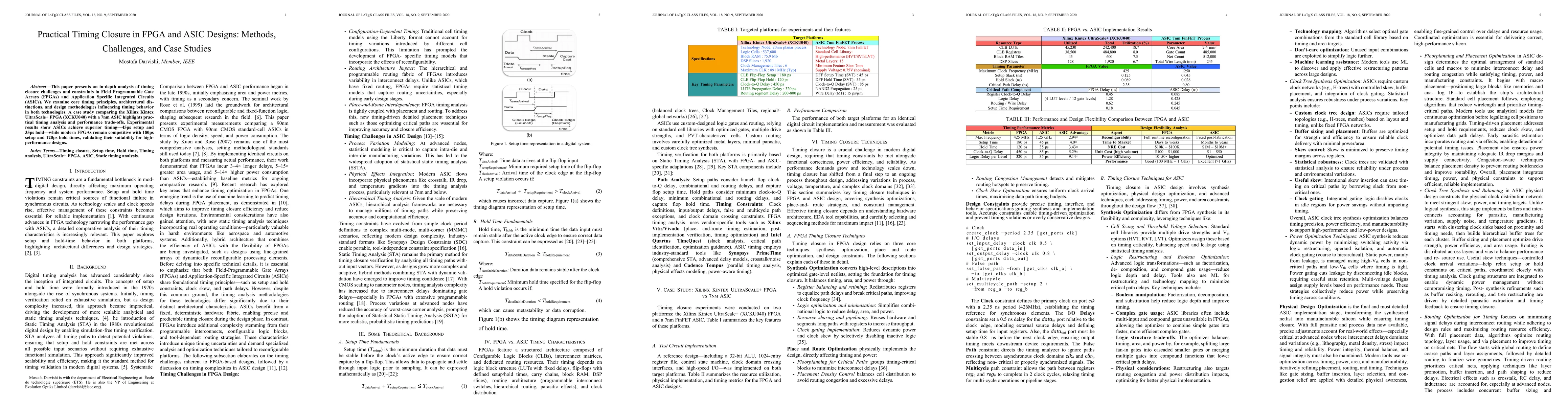
This paper presents an in-depth analysis of timing closure challenges and constraints in Field Programmable Gate Arrays (FPGAs) and Application Specific Integrated Circuits (ASICs). We examine core timing principles, architectural distinctions, and design methodologies influencing timing behavior in both technologies. A case study comparing the Xilinx Kintex UltraScale+ FPGA (XCKU040) with a 7nm ASIC highlights practical timing analysis and performance trade-offs. Experimental results show ASICs achieve superior timing of 45ps setup and 35ps hold, while modern FPGAs remain competitive with 180ps setup and 120ps hold times, validating their suitability for high-performance designs.

AI Key Findings

Generated Nov 08, 2025

Methodology — What approach did the authors take?

The research employs a comparative analysis of FPGA and ASIC design methodologies, focusing on timing closure techniques, power management strategies, and process variation mitigation across technology scaling nodes.

Key Results — What are the main findings?

  • ASICs achieve tighter timing margins (60 units at 22nm) compared to FPGAs
  • Dynamic power dominates at 180nm but static power becomes critical at 22nm
  • Process variations increase exponentially as technology scales from 180nm to 22nm

Significance — Why does this research matter?

This study highlights critical design challenges at advanced nodes, providing insights for developing more robust and power-efficient digital systems in next-generation semiconductor technologies.

Technical Contribution — What is the technical contribution?

Provides a comprehensive analysis of technology scaling impacts on timing closure, power consumption, and process variation across FPGA and ASIC design domains.

Novelty — What is new about this work?

First systematic comparison of timing margin degradation and power consumption evolution across multiple technology nodes, combined with practical design recommendations for advanced node implementations.

Limitations — What are the limitations of this study?

  • Data primarily based on simulation results rather than physical prototypes
  • Analysis focuses on specific nodes (180nm-22nm) without broader industry context

Future Work — What did the authors propose for future work?

  • Developing adaptive timing methodologies for real-time process variation compensation
  • Exploring hybrid design approaches combining FPGA and ASIC benefits
  • Investigating long-term reliability under aging effects

Paper Details

Paper ID: 2510.26985
Comments: 5 figures, 3 tables
Categories:
cs.AR eess.SP

How to Cite This Paper

BibTeX
@article{darvishi2025practical,
  title         = {Practical Timing Closure in FPGA and ASIC Designs: Methods, Challenges,
  and Case Studies},
  author        = {Darvishi, Mostafa},
  year          = {2025},
  eprint        = {2510.26985},
  archivePrefix = {arXiv},
  primaryClass  = {cs.AR},
}
APA 7
Darvishi, M. (2025). Practical Timing Closure in FPGA and ASIC Designs: Methods, Challenges,
  and Case Studies. arXiv. https://arxiv.org/abs/2510.26985
MLA 9
Darvishi, Mostafa. "Practical Timing Closure in FPGA and ASIC Designs: Methods, Challenges,
  and Case Studies." arXiv, 2025, arxiv.org/abs/2510.26985.

Comments (0)

This website uses cookies to ensure you get the best experience. Learn more