Precise nanoscale temperature mapping in operational microelectronic devices by use of a phase change material
Publication
Metrics
Paper Preview
Abstract
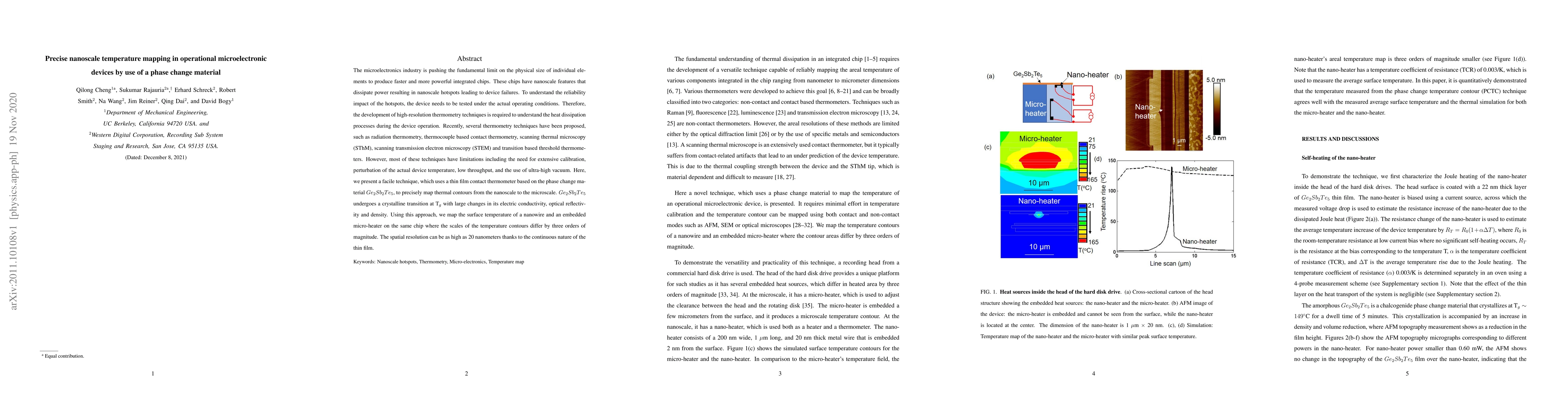
The microelectronics industry is pushing the fundamental limit on the physical size of individual elements to produce faster and more powerful integrated chips. These chips have nanoscale features that dissipate power resulting in nanoscale hotspots leading to device failures. To understand the reliability impact of the hotspots, the device needs to be tested under the actual operating conditions. Therefore, the development of high-resolution thermometry techniques is required to understand the heat dissipation processes during the device operation. Recently, several thermometry techniques have been proposed,such as radiation thermometry, thermocouple based contact thermometry, scanning thermal microscopy (SThM), scanning transmission electron microscopy (STEM) and transition based threshold thermometers. However, most of these techniques have limitations including the need for extensive calibration, perturbation of the actual device temperature, low throughput, and the use of ultra-high vacuum. Here, we present a facile technique, which uses a thin film contact thermometer based on the phase change material Ge2Sb2Te5, to precisely map thermal contours from the nanoscale to the microscale. Ge2Sb2Te5 undergoes a crystalline transition at Tg with large changes in its electric conductivity, optical reflectivity and density. Using this approach, we map the surface temperature of a nanowire and an embedded micro-heater on the same chip where the scales of the temperature contours differ by three orders of magnitude. The spatial resolution can be as high as 20 nanometers thanks to the continuous nature of the thin film.
AI Key Findings
Get AI-generated insights about this paper's methodology, results, significance, and more — seven facets brought into focus.
Impact
Paper Details
Authors
PDF Preview
Key Terms
Citation Network
Current paper (gray), citations (green), references (blue)
Display is limited for performance on very large graphs.
Discussion 0