ArxivLens

Publication

Published: Sep 10, 2025
Categories: cs.HC

Metrics

Source: ArXiv

Quick Answers

What methodology did the authors use?

The study combines 3D printing with embedded electronics by integrating PCBs into the printing process using Prinjection. This involves slicing designs, inserting PCBs mid-print, and using conductive filaments for sensor structures and connections while keeping digital interconnections on traditional PCBs. More in Methodology →

What are the key results?

Prinjection enables robust integration of electronics within 3D printed objects — PCBs can be recovered and recycled through heating and mechanical separation More in Key Results →

Why is this work significant?

This research bridges the gap between digital fabrication and physical electronics, enabling the creation of fully functional interactive devices that are both durable and recyclable, which has implications for sustainable manufacturing and personalized electronics production. More in Significance →

What are the main limitations?

The process requires specialized tools for PCB insertion and recovery — High resistance of conductive filaments may limit certain applications More in Limitations →

Paper Preview

Abstract

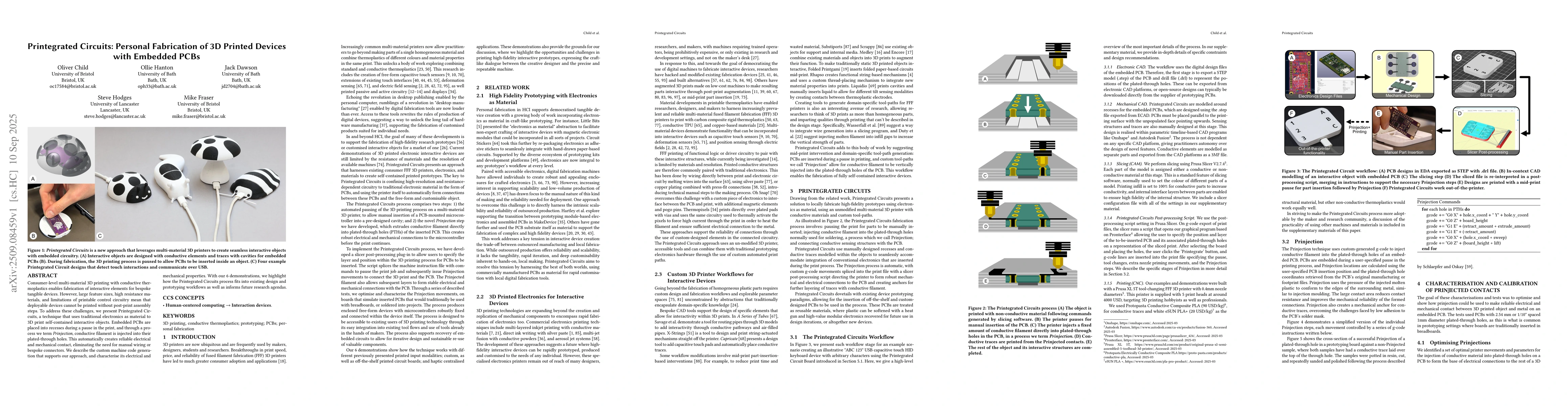
Consumer-level multi-material 3D printing with conductive thermoplastics enables fabrication of interactive elements for bespoke tangible devices. However, large feature sizes, high resistance materials, and limitations of printable control circuitry mean that deployable devices cannot be printed without post-print assembly steps. To address these challenges, we present Printegrated Circuits, a technique that uses traditional electronics as material to 3D print self-contained interactive objects. Embedded PCBs are placed into recesses during a pause in the print, and through a process we term \textit{Prinjection}, conductive filament is injected into their plated-through holes. This automatically creates reliable electrical and mechanical contact, eliminating the need for manual wiring or bespoke connectors. We describe the custom machine code generation that supports our approach, and characterise its electrical and mechanical properties. With our 6 demonstrations, we highlight how the Printegrated Circuits process fits into existing design and prototyping workflows as well as informs future research agendas.
Key Findings, in focus

Seven facets of this paper, analysed and brought into focus by AI.

AI-generated · verify against source Generated Nov 02, 2025
In focus · one-line synthesis

This research bridges the gap between digital fabrication and physical electronics, enabling the creation of fully functional interactive devices that are both durable and recyclable, which has implications for sustainable manufacturing and personalized electronics production.

01
MethodologyHow they did it

The study combines 3D printing with embedded electronics by integrating PCBs into the printing process using Prinjection. This involves slicing designs, inserting PCBs mid-print, and using conductive filaments for sensor structures and connections while keeping digital interconnections on traditional PCBs.

02
ResultsWhat they found
  • Prinjection enables robust integration of electronics within 3D printed objects
  • PCBs can be recovered and recycled through heating and mechanical separation
  • Conductive and non-conductive PLA can be shredded and re-extruded into new filaments
03
SignificanceWhy it matters

This research bridges the gap between digital fabrication and physical electronics, enabling the creation of fully functional interactive devices that are both durable and recyclable, which has implications for sustainable manufacturing and personalized electronics production.

04
Technical ContributionsWhat's new technically

A novel method for embedding PCBs into 3D printing workflows using Prinjection, allowing for both functional electronics integration and material recovery

05
NoveltyWhat sets it apart

The integration of PCBs with 3D printing through Prinjection, combined with material recovery processes, represents a significant advancement in personal fabrication by enabling sustainable, fully functional interactive devices

06
LimitationsWhat to be cautious about
  • The process requires specialized tools for PCB insertion and recovery
  • High resistance of conductive filaments may limit certain applications
07
Future WorkWhere it goes next
  • Exploring more conductive materials for better performance
  • Developing flexible and extendable tools for design workflows
  • Investigating biodegradable materials for sustainable fabrication

Paper Details

Paper ID: 2509.08459
Categories:
cs.HC

How to Cite This Paper

Reference manager: RIS EndNote


Discussion 0

This website uses cookies to ensure you get the best experience. Learn more