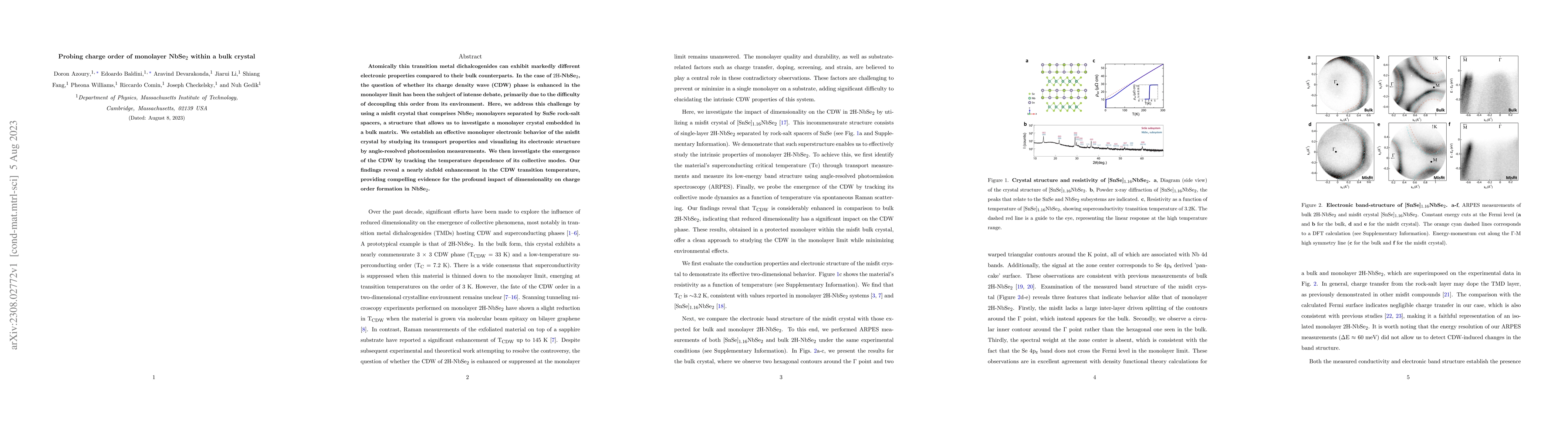
Probing charge order of monolayer NbSe$_2$ within a bulk crystal
Publication
Metrics
AI Quick Summary
This study investigates the charge density wave (CDW) phase in monolayer NbSe$_2$ within a bulk crystal using a misfit crystal structure. The research reveals a nearly sixfold increase in the CDW transition temperature, demonstrating the significant influence of reduced dimensionality on charge order formation in NbSe$_2$.
Paper Preview
Abstract
Atomically thin transition metal dichalcogenides can exhibit markedly different electronic properties compared to their bulk counterparts. In the case of NbSe$_2$, the question of whether its charge density wave (CDW) phase is enhanced in the monolayer limit has been the subject of intense debate, primarily due to the difficulty of decoupling this order from its environment. Here, we address this challenge by using a misfit crystal that comprises NbSe$_2$ monolayers separated by SnSe rock-salt spacers, a structure that allows us to investigate a monolayer crystal embedded in a bulk matrix. We establish an effective monolayer electronic behavior of the misfit crystal by studying its transport properties and visualizing its electronic structure by angle-resolved photoemission measurements. We then investigate the emergence of the CDW by tracking the temperature dependence of its collective modes. Our findings reveal a nearly sixfold enhancement in the CDW transition temperature, providing compelling evidence for the profound impact of dimensionality on charge order formation in NbSe$_2$.
AI Key Findings
Get AI-generated insights about this paper's methodology, results, significance, and more — seven facets brought into focus.
Impact
Paper Details
Authors
PDF Preview
Key Terms
Citation Network
Current paper (gray), citations (green), references (blue)
Display is limited for performance on very large graphs.
Discussion 0