Probing lattice vibration at surface and interface of SiO$_2$/Si with nanometer resolution
Publication
Metrics
AI Quick Summary
This study employs advanced electron microscopy to probe lattice vibrations at the surface and interface of SiO$_2$/Si with nanometer resolution, revealing distinct sub-modes: surface, bulk, and interface modes. The surface modes exhibit a thickness-dependent blue-shift, while bulk modes increase linearly with film thickness, providing insights into bonding conditions that could enhance silicon-based device design.
Paper Preview
Abstract
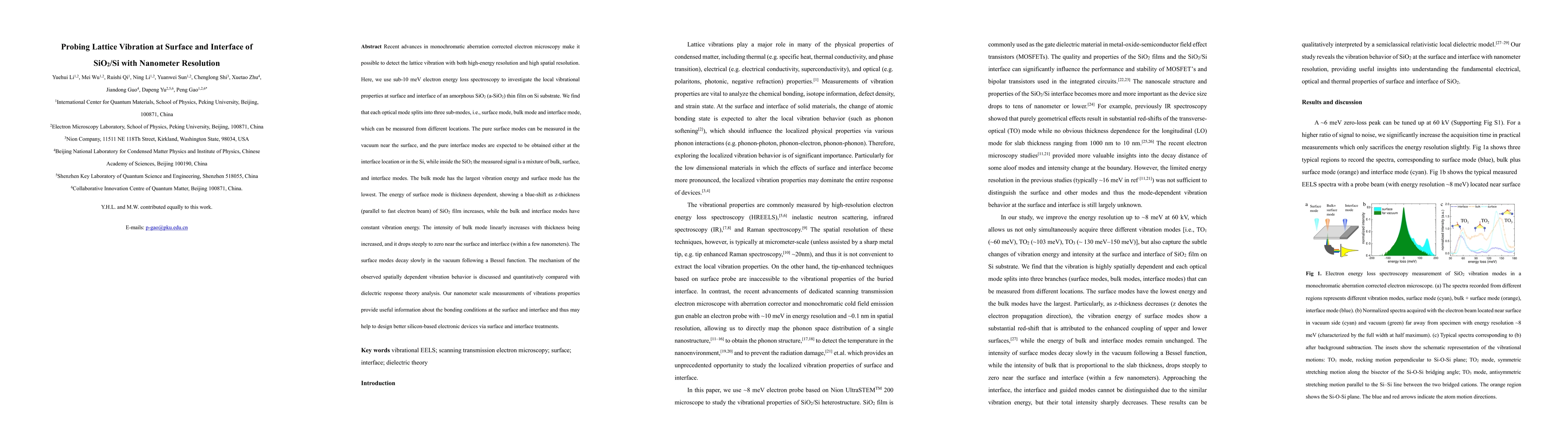
Recent advances in monochromatic aberration corrected electron microscopy make it possible to detect the lattice vibration with both high-energy resolution and high spatial resolution. Here, we use sub-10 meV electron energy loss spectroscopy to investigate the local vibrational properties at surface and interface of an amorphous SiO$_2$ (a-SiO$_2$) thin film on Si substrate. We find that each optical mode splits into three sub-modes, i.e., surface mode, bulk mode and interface mode, which can be measured from different locations. The pure surface modes can be measured in the vacuum near the surface, and the pure interface modes are expected to be obtained either at the interface location or in the Si, while inside the SiO$_2$ the measured signal is a mixture of bulk, surface, and interface modes. The bulk mode has the largest vibration energy and surface mode has the lowest. The energy of surface mode is thickness dependent, showing a blue-shift as z-thickness (parallel to fast electron beam) of SiO$_2$ film increases, while the bulk and interface modes have constant vibration energy. The intensity of bulk mode linearly increases with thickness being increased, and it drops steeply to zero near the surface and interface (within a few nanometers). The surface modes decay slowly in the vacuum following a Bessel function. The mechanism of the observed spatially dependent vibration behavior is discussed and quantitatively compared with dielectric response theory analysis. Our nanometer scale measurements of vibrations properties provide useful information about the bonding conditions at the surface and interface and thus may help to design better silicon-based electronic devices via surface and interface treatments
AI Key Findings
Get AI-generated insights about this paper's methodology, results, significance, and more — seven facets brought into focus.
Impact
Paper Details
PDF Preview
Key Terms
Citation Network
Current paper (gray), citations (green), references (blue)
Display is limited for performance on very large graphs.
Discussion 0