This paper presents a novel method for precise, non-contact temperature measurement at the nanoscale using scanning precession electron diffraction in transmission electron microscopy. The technique reveals temperature and thermal vibration mapping in graphene with high spatial resolution, offering insights into the effects of lattice parameters and thickness on vibrational properties.
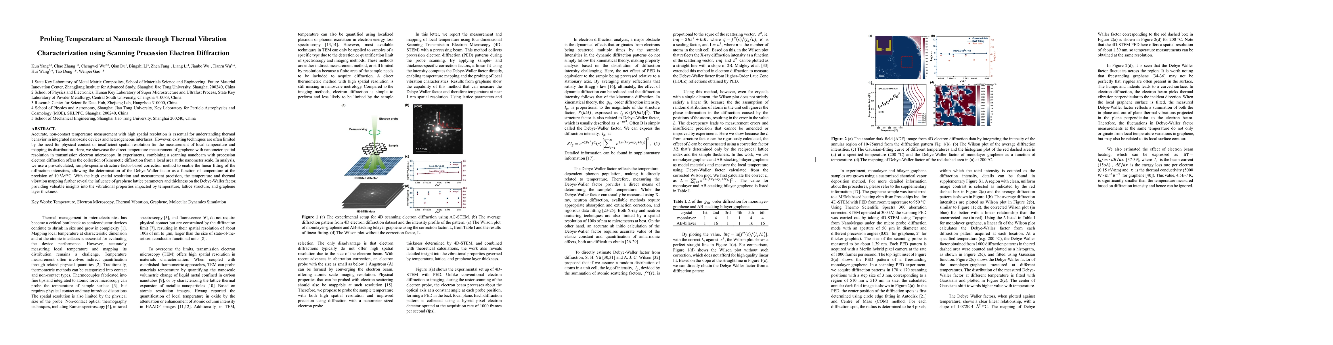
Accurate, non-contact temperature measurement with high spatial resolution is essential for understanding thermal behavior in integrated nanoscale devices and heterogeneous interfaces. However, existing techniques are often limited by the need for physical contact or insufficient spatial resolution for the measurement of local temperature and mapping its distribution. Here, we showcase the direct temperature measurement of graphene with nanometer spatial resolution in transmission electron microscopy. In experiments, combining a scanning nanobeam with precession electron diffraction offers the collection of kinemetic diffraction from a local area at the nanometer scale. In analysis, we use a pre-calculated, sample-specific structure-factor-based correction method to enable the linear fitting of the diffraction intensities, allowing the determination of the Debye-Waller factor as a function of temperature at the precision of 10-4{\AA}2/{\deg}C. With the high spatial resolution and measurement precision, the temperature and thermal vibration mapping further reveal the influence of graphene lattice parameters and thickness on the Debye-Waller factor, providing valuable insights into the vibrational properties impacted by temperature, lattice structure, and graphene layer thickness.
Generated Jun 09, 2025
The research employs Scanning Precession Electron Diffraction (PEd) combined with a transmission electron microscopy (TEM) setup to measure temperature at the nanoscale. This method corrects dynamical effects in electron diffraction patterns, allowing for kinematical analysis and determination of the Debye-Waller factor with high precision.
This research is significant as it provides a non-contact, high-resolution method for temperature measurement at the nanoscale, crucial for understanding thermal behavior in integrated nanoscale devices and heterogeneous interfaces. It overcomes limitations of existing techniques by offering precise temperature mapping with spatial resolution down to single nanometers.
The paper introduces a sample-specific structure-factor-based correction method to enable linear fitting of diffraction intensities, allowing precise determination of the Debye-Waller factor from electron diffraction data.
The novelty of this work lies in its application of Scanning Precession Electron Diffraction combined with a corrected Wilson plot to measure the Debye-Waller factor with high precision and nanoscale resolution, providing insights into vibrational properties influenced by temperature, lattice structure, and material thickness.
No key terms available for this paper.
Current paper (gray), citations (green), references (blue)
No citations found for this paper.
Comments (0)