Processing of Photonic Crystal Nanocavity for Quantum Information in Diamond
Publication
Metrics
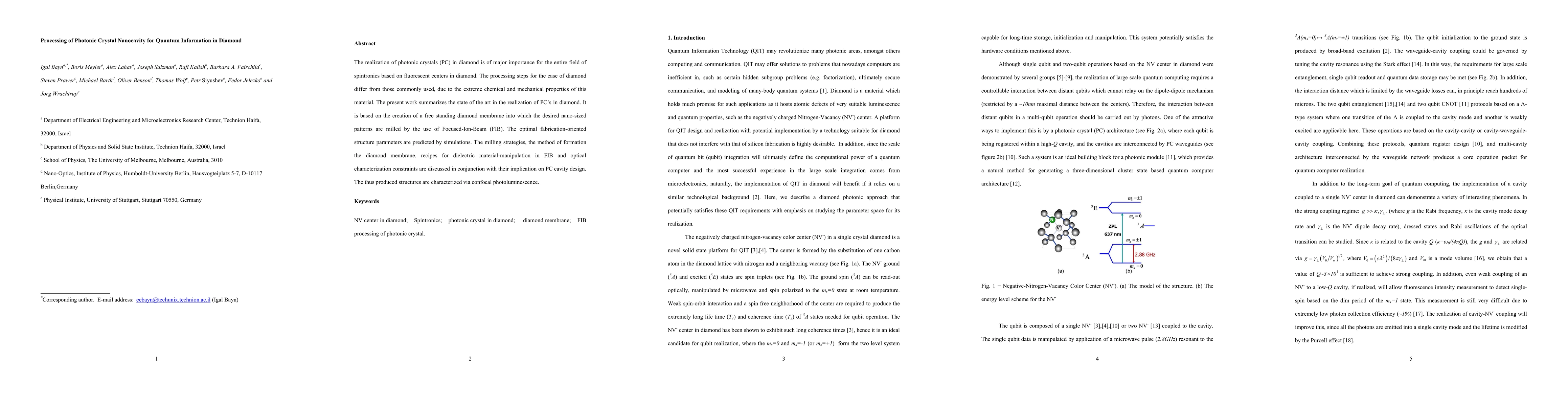
AI Quick Summary
This paper details the fabrication of photonic crystal nanocavities in diamond using Focused-Ion-Beam milling, emphasizing unique processing strategies due to diamond's properties. The study combines simulation-guided structural parameters and optical characterization to optimize cavity design for quantum information applications in spintronics.
Paper Preview
Abstract
The realization of photonic crystals (PC) in diamond is of major importance for the entire field of spintronics based on fluorescent centers in diamond. The processing steps for the case of diamond differ from those commonly used, due to the extreme chemical and mechanical properties of this material. The present work summarizes the state of the art in the realization of PC's in diamond. It is based on the creation of a free standing diamond membrane into which the desired nano-sized patterns are milled by the use of Focused-Ion-Beam (FIB). The optimal fabrication-oriented structure parameters are predicted by simulations. The milling strategies, the method of formation the diamond membrane, recipes for dielectric material-manipulation in FIB and optical characterization constraints are discussed in conjunction with their implication on PC cavity design. The thus produced structures are characterized via confocal photoluminescence.
AI Key Findings
Get AI-generated insights about this paper's methodology, results, significance, and more — seven facets brought into focus.
Impact
Paper Details
PDF Preview
Key Terms
Citation Network
Current paper (gray), citations (green), references (blue)
Display is limited for performance on very large graphs.
Discussion 0