Summary
Meta-optics, the application of metasurfaces into optical systems, is seeing an accelerating development owing to advantages in size, weight and cost and the ability to program optical functions beyond traditional refractive optics. The transition of meta-optics from the laboratory into applications is enabled by scalable production methods based on highly reproducible semiconductor process technology. Here, we introduce a novel method for fabrication of double-sided metasurfaces through deep-UV lithography as a production-ready method for achieving high-quality meta-optics. We achieve patterning of a silicon wafer on both sides with mutual alignment of around 25 $\mu$m based on tool accuracy, without requiring through-wafer alignment markers other than the wafer notch. A first novel application highlighting the benefits of double-sided design is demonstrated in the form of a dual-band metalens with independent control over focal lengths in mid- and long-wave infrared bands. Using multi-reticle stitching we demonstrate a 40 mm diameter, large-area metalens with excellent broadband imaging performance, showing partial cancelling of chromatic dispersion when used in a hybrid configuration with a BaF$_2$ refractive lens. Our work opens new avenues for infrared meta-optics designs and double-side meta-optics fabrication through a production-ready technique which can be directly translated into scalable technology for real-world applications.
AI Key Findings
Generated Jun 08, 2025
Methodology
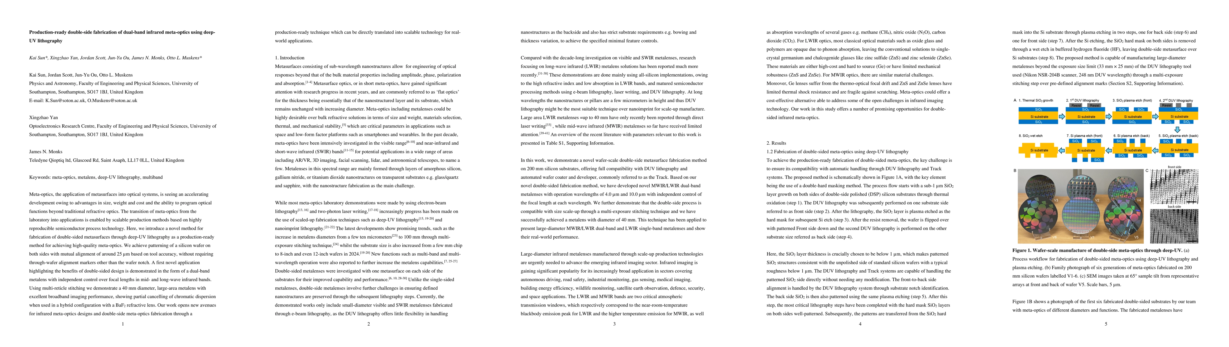
The research introduces a novel method for fabrication of double-sided metasurfaces through deep-UV lithography, achieving patterning of a silicon wafer on both sides with mutual alignment of around 25 µm without requiring through-wafer alignment markers other than the wafer notch.
Key Results
- A production-ready fabrication method for high-quality meta-optics is demonstrated.
- A dual-band metalens with independent control over focal lengths in mid- and long-wave infrared bands is presented.
- A 40 mm diameter, large-area metalens with excellent broadband imaging performance is achieved, showing partial cancelling of chromatic dispersion when used in a hybrid configuration with a BaF2 refractive lens.
Significance
This work opens new avenues for infrared meta-optics designs and double-side meta-optics fabrication through a production-ready technique, which can be directly translated into scalable technology for real-world applications.
Technical Contribution
The introduction of a novel double-sided fabrication method using deep-UV lithography for meta-optics, enabling independent control over focal lengths in dual-band infrared applications.
Novelty
This research presents a production-ready double-sided fabrication method for meta-optics, distinct from previous laboratory-scale techniques, by leveraging semiconductor process technology and deep-UV lithography.
Limitations
- The paper does not discuss potential limitations of the deep-UV lithography method in terms of resolution or throughput for large-scale production.
- No comparison is provided with existing fabrication methods regarding cost or complexity.
Future Work
- Investigate the scalability of the method for mass production of meta-optics.
- Explore the applicability of the technique to other wavelength ranges or optical systems.
Paper Details
PDF Preview
Citation Network
Current paper (gray), citations (green), references (blue)
Display is limited for performance on very large graphs.
Similar Papers
Found 4 papersGeneric Lithography Modeling with Dual-band Optics-Inspired Neural Networks
Anima Anandkumar, Haoxing Ren, Haoyu Yang et al.
Partially coherent double phase holography in visible using meta-optics
Arka Majumdar, Steven Brunton, Johannes E. Froech et al.
No citations found for this paper.
Comments (0)