This paper investigates the structural and electrical properties of Al2O3 and HfO2 dielectric oxides grown by Atomic Layer Deposition (ALD) for Metal-Insulator-Semiconductor (MIS) structures. The 40-100 nm thick layers show excellent surface flatness and amorphous structure, enabling effective metallic gate integration and achieving low leakage currents below 1 nA at 3 MV/cm at 77 K.
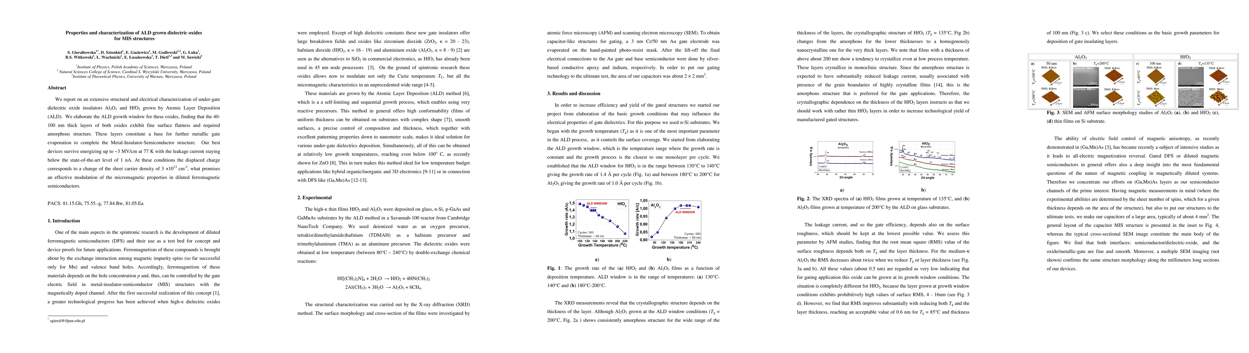
We report on an extensive structural and electrical characterization of under-gate dielectric oxide insulators Al2O3 and HfO2 grown by Atomic Layer Deposition (ALD). We elaborate the ALD growth window for these oxides, finding that the 40-100 nm thick layers of both oxides exhibit fine surface flatness and required amorphous structure. These layers constitute a base for further metallic gate evaporation to complete the Metal-Insulator-Semiconductor structure. Our best devices survive energizing up to ~3 MV/cm at 77 K with the leakage current staying below the state-of-the-art level of 1 nA. At these conditions the displaced charge corresponds to a change of the sheet carrier density of 3 \times 1013 cm-2, what promises an effective modulation of the micromagnetic properties in diluted ferromagnetic semiconductors.
Get AI-generated insights about this paper's methodology, results, and significance.
Current paper (gray), citations (green), references (blue)
Susan Trolier-McKinstry, Pedram Yousefian, Betul Akkopru-Akgun et al.
Mansour Aouassa, Saud Algarni, Ibrahim Althobaiti et al.
Title | Authors | Year | Actions |
---|---|---|---|
Ceramic thin-film composite membranes with tunable subnanometer pores for molecular sieving
|
Xuechen Zhou, Rahul Shevate, Dahong Huang, Tianchi Cao, Xin Shen, Shu Hu, A. Mane, Jeffrey W. Elam, Jaehong Kim, M. Elimelech
|
2023
|
View Paper |
Influence of growth temperature on dielectric strength of Al2O3 thin films prepared via atomic layer deposition at low temperature
|
Suyeon Kim, Seunghwa Lee, In-Ho Jo, Jongsu Seo, Y. Yoo, Jeong Hwan Kim
|
2022
|
View Paper |
Alumina Graphene Catalytic Condenser for Programmable Solid Acids
|
T. Onn, Sallye R. Gathmann, Yuxin Wang, R. Patel, Silu Guo, Han Chen, Jimmy K. Soeherman, P. Christopher, Geoffrey A. Rojas, K. Mkhoyan, M. Neurock, O. Abdelrahman, C. Frisbie, Paul J. Dauenhauer
|
2022
|
View Paper |
Impact of blocking layer on DSSC performance based on new dye -indolo[3,2,1-jk]carbazole derivative and N719
|
Paweł Gnida, Aneta Slodek, P. Chulkin, M. Vasylieva, A. Pająk, A. Seweryn, M. Godlewski, B. Witkowski, Grażyna Szafraniec-Gorol, E. Schab-Balcerzak
|
2022
|
View Paper |
Investigations of Structural and Electrical Properties of ALD Films Formed with the Ozone Precursor
|
A. Seweryn, K. Lawniczak-Jablonska, P. Kuźmiuk, S. Gierałtowska, M. Godlewski, R. Mroczyński
|
2021
|
View Paper |
Synthesis of Al/HfO2/p-Si Schottky diodes and the investigation of their electrical and dielectric properties
|
I. Er, A. O. Çağırtekin, Murat Artuç, S. Acar
|
2021
|
View Paper |
Voltage control of spin–orbit torque in Pd/Co/Pd/HfO x
|
T. Hirai, Y. Hibino, Kento Hasegawa, M. Kohda, T. Koyama, D. Chiba
|
2020
|
View Paper |
Importance of precursor delivery mechanism for Tetra-kis-ethylmethylaminohafnium/water atomic layer deposition process
|
S. Tomer, Vandana, Jagannath Panigrahi, R. Srivastava, C. Rauthan
|
2019
|
View Paper |
Electrical characteristics of vertical-geometry Schottky junction to magnetic insulator (Ga,Mn)N heteroepitaxially grown on sapphire
|
K. Kalbarczyk, K. Dybko, K. Gas, D. Sztenkiel, M. Foltyn, M. Majewicz, P. Nowicki, E. Łusakowska, D. Hommel, M. Sawicki
|
2019
|
View Paper |
Hole and electron trapping in HfO2/Al2O3 nanolaminated stacks for emerging non-volatile flash memories
|
D. Spassov, A. Paskaleva, T. Krajewski, E. Guziewicz, G. Luka
|
2018
|
View Paper |
Étude des potentialités de la transduction diélectrique de haute permittivité pour les résonateurs NEMS et MEMS
|
Cécile Fuinel
|
2018
|
View Paper |
Atomic layer deposition of sub-10 nm high-K gate dielectrics on top-gated MoS2 transistors without surface functionalization
|
Yu-Shu Lin, Po-Hsien Cheng, K. Huang, Hsin-Chih Lin, Miin-Jang Chen
|
2018
|
View Paper |
Electric-field-induced magnetic domain writing in a Co wire
|
Yuki Tanaka, T. Hirai, T. Koyama, D. Chiba
|
2018
|
View Paper |
Control of magnetism by electrical charge doping or redox reactions in a surface-oxidized Co thin film with a solid-state capacitor structure
|
T. Hirai, T. Koyama, D. Chiba
|
2018
|
View Paper |
Hydrophobicity of Rare Earth Oxides Grown by Atomic Layer Deposition
|
I. Oh, Kan-San Kim, Zonghoon Lee, K. Ko, C. Lee, Su Jeong Lee, Jae Min Myung, Clément Lansalot-Matras, Wontae Noh, C. Dussarrat, Hyungjun Kim, Han‐Bo‐Ram Lee
|
2015
|
View Paper |
Roll-to-Roll Atmospheric Atomic Layer Deposition of Al2O3 Thin Films on PET Substrates†
|
K. Ali, K. Choi, N. Muhammad
|
2014
|
View Paper |
Nonlocal resistance and its fluctuations in microstructures of band-inverted HgTe/(Hg,Cd)Te quantum wells
|
G. Grabecki, J. Wr'obel, M. Czapkiewicz, L. Cywi'nski, S. Gierałtowska, E. Guziewicz, M. Zholudev, V. Gavrilenko, N. Mikhailov, S. Dvoretski, F. Teppe, W. Knap, T. Dietl
|
2013
|
View Paper |
Thin Films of High‐k Oxides and ZnO for Transparent Electronic Devices
|
S. Gierałtowska, L. Wachnicki, B. Witkowski, E. Guziewicz, M. Godlewski
|
2013
|
View Paper |
Application of deposited by ALD HfO2 and Al2O3 layers in double-gate dielectric stacks for non-volatile semiconductor memory (NVSM) devices
|
R. Mroczyński, A. Taube, S. Gierałtowska, E. Guziewicz, M. Godlewski
|
2012
|
View Paper |
ALD grown zinc oxide with controllable electrical properties
|
E. Guziewicz, M. Godlewski, L. Wachnicki, T. Krajewski, G. Luka, S. Gierałtowska, R. Jakieła, A. Stonert, W. Lisowski, M. Krawczyk, J. Sobczak, A. Jablonski
|
2012
|
View Paper |
Atomic layer deposition grown composite dielectric oxides and ZnO for transparent electronic applications
|
S. Gierałtowska, L. Wachnicki, B. Witkowski, M. Godlewski, E. Guziewicz
|
2012
|
View Paper |
Electrical characterization of HfO2 based omega finfet compared with conventional SiO2 material
|
K. J. Swabhijit, J. Mohana
|
2023
|
View Paper |
Evaluation of ALD Oxides as the Sensing Layer for Ion Sensors
|
Elis Nycander
|
2016
|
View Paper |
THREE DIMENSIONAL NANOPLASMONIC SURFACES : MODELING , FABRICATION AND CHARACTERIZATION
|
Kıvanç Güngör
|
2013
|
View Paper |
Properties of thin films of high-k oxides grown by atomic layer deposition at low temperature for electronic applications
|
S. Gierałtowska, Ł. Wachnicki, B. Witkowski, M. Godlewski, E. Guziewicz
|
2013
|
View Paper |
Tlenki dielektryczne wytwarzane metodą osadzania warstw atomowych w niskich temperaturach dla zastosowań w elektronice jako izolatory
|
S. Gieraltowska, Łukasz Wachnicki, Bartlomiej S. Witkowski, M. Godlewski, E. Guziewicz
|
2012
|
View Paper |
Comments (0)