Quantification of nanoscale density fluctuations in hydrogenated amorphous silicon
Publication
Metrics
AI Quick Summary
Researchers used SAXS and SANS to study hydrogenated amorphous silicon, discovering two phases: 1.2nm voids and dense ordered domains with an average diameter of 1nm, which affect the material's structure and electronic properties.
Paper Preview
Abstract
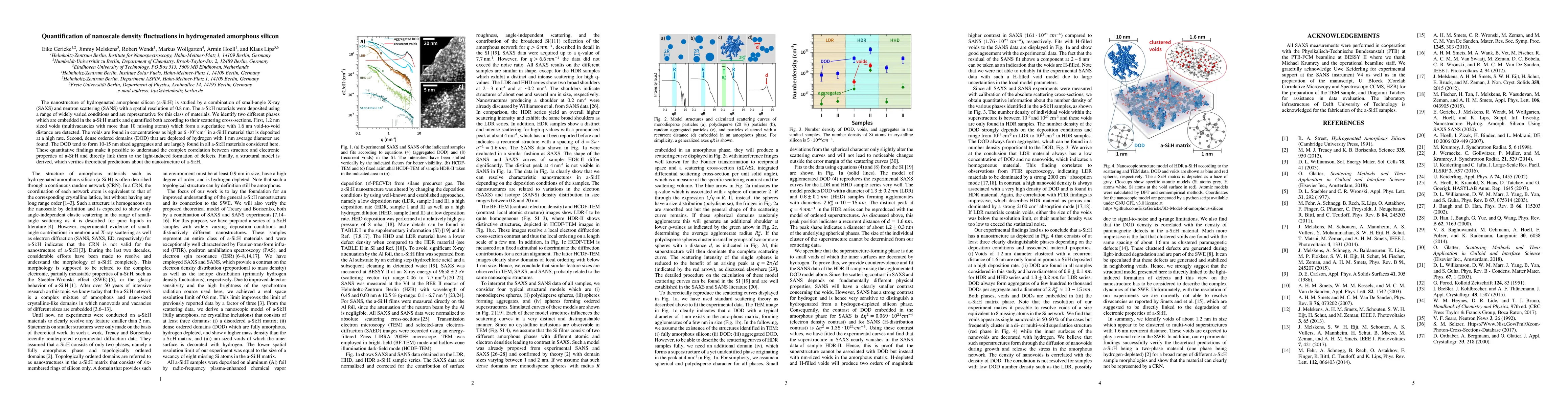
The nanostructure of hydrogenated amorphous silicon (a Si:H) is studied by a combination of small-angle X-ray (SAXS) and neutron scattering (SANS) with a spatial resolution of 0.8 nm. The a-Si:H materials were deposited using a range of widely varied conditions and are representative for this class of materials. We identify two different phases which are embedded in the a-Si:H matrix and quantified both according to their scattering cross-sections. First, 1.2 nm sized voids (multivacancies with more than 10 missing atoms) which form a superlattice with 1.6 nm void-to-void distance are detected. The voids are found in concentrations as high as 6*10^19 ccm in a-Si:H material that is deposited at a high rate. Second, dense ordered domains (DOD) that are depleted of hydrogen with 1 nm average diameter are found. The DOD tend to form 10-15 nm sized aggregates and are largely found in all a-Si:H materials considered here. These quantitative findings make it possible to understand the complex correlation between structure and electronic properties of a-Si:H and directly link them to the light-induced formation of defects. Finally, a structural model is derived, which verifies theoretical predictions about the nanostructure of a-Si:H.
AI Key Findings
Get AI-generated insights about this paper's methodology, results, significance, and more — seven facets brought into focus.
Impact
Paper Details
PDF Preview
Key Terms
Citation Network
Current paper (gray), citations (green), references (blue)
Display is limited for performance on very large graphs.
Discussion 0