01
MethodologyHow they did it
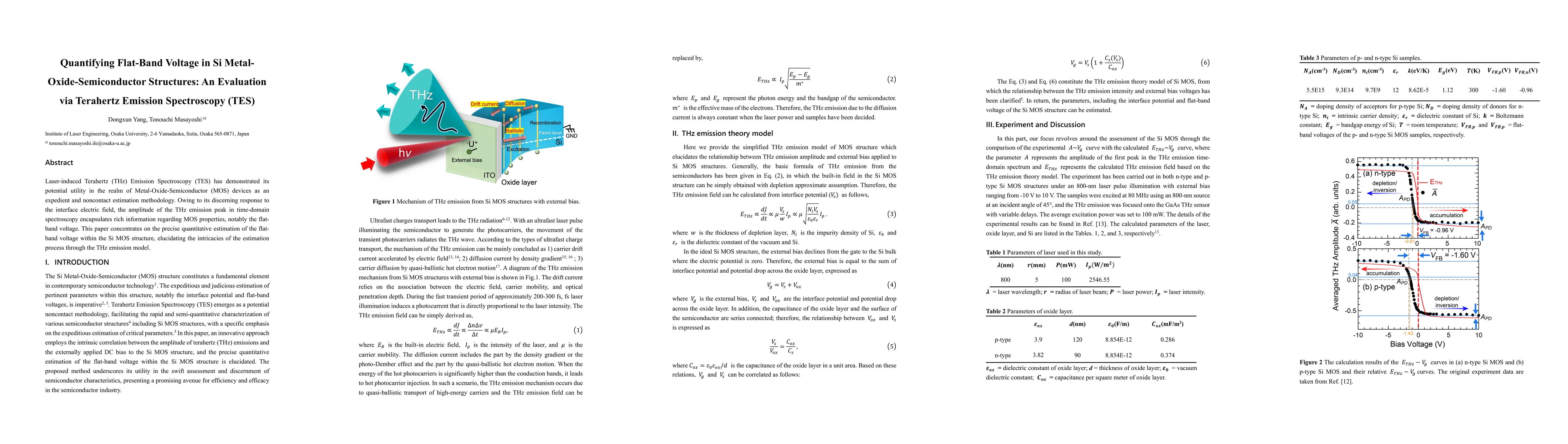
The research employs Laser-induced Terahertz (THz) Emission Spectroscopy (TES) to estimate flat-band voltage in Si Metal-Oxide-Semiconductor (MOS) structures non-contactingly and expeditiously by analyzing the amplitude of the THz emission peak in time-domain spectroscopy, which correlates with MOS properties, especially flat-band voltage.
Discussion 0