01
MethodologyHow they did it
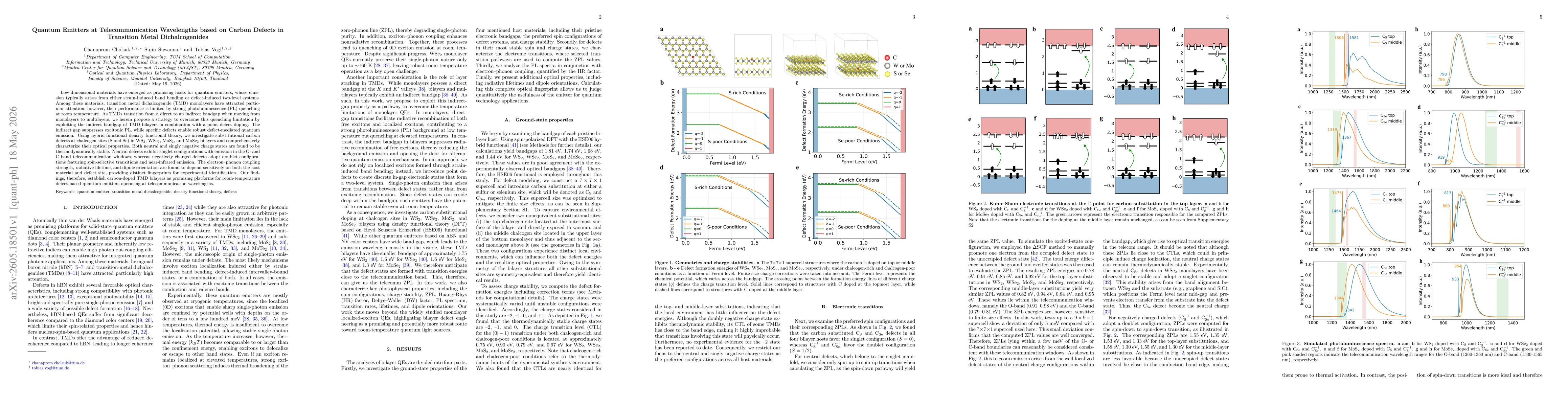
The study employs hybrid-functional density functional theory (HSE06) to model carbon substitutions at chalcogen sites (S and Se) in WS2, WSe2, MoS2, and MoSe2 bilayers. A 7×7×1 supercell is used to minimize finite-size effects, with two inequivalent defect configurations (top surface and middle layer) to capture environmental influences. Defect formation energies and charge transition levels are computed with appropriate corrections; spin states and optical transitions are analyzed to predict ZPL energies, Huang–Rhys factors, Debye–Waller factors, radiative lifetimes, and dipole orientations. Temperature considerations are addressed by focusing on room-temperature stability of defect states in bilayer hosts with indirect bandgaps.
Discussion 0