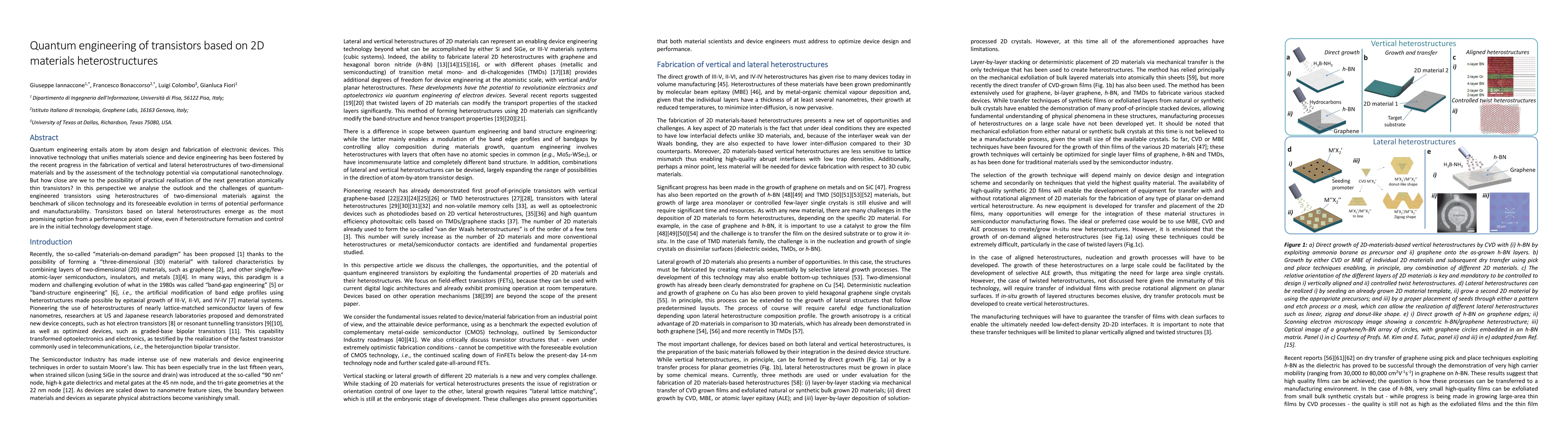
Quantum engineering of transistors based on 2D materials heterostructures
Publication
Metrics
AI Quick Summary
Researchers analyze the potential of quantum-engineered transistors using 2D materials heterostructures, finding that lateral heterostructures offer promising performance despite initial challenges in formation and control. The study compares these transistors to silicon technology and its future evolution.
Paper Preview
Abstract
Quantum engineering entails atom by atom design and fabrication of electronic devices. This innovative technology that unifies materials science and device engineering has been fostered by the recent progress in the fabrication of vertical and lateral heterostructures of two-dimensional materials and by the assessment of the technology potential via computational nanotechnology. But how close are we to the possibility of practical realisation of the next generation atomically thin transistors? In this perspective we analyse the outlook and the challenges of quantum- engineered transistors using heterostructures of two-dimensional materials against the benchmark of silicon technology and its foreseeable evolution in terms of potential performance and manufacturability. Transistors based on lateral heterostructures emerge as the most promising option from a performance point of view, even if heterostructure formation and control are in the initial technology development stage.
AI Key Findings
Get AI-generated insights about this paper's methodology, results, significance, and more — seven facets brought into focus.
Impact
Paper Details
PDF Preview
Key Terms
Citation Network
Current paper (gray), citations (green), references (blue)
Display is limited for performance on very large graphs.
Discussion 0