Quantum enhanced electric field mapping within semiconductor devices
Publication
Metrics
AI Quick Summary
This paper proposes a novel quantum-enhanced technique using silicon vacancy centers in 4H-SiC to map the 3D electric field and free charge carrier concentrations within silicon carbide semiconductor devices. The method employs Stark shift measurements via photoluminescence excitation to achieve nanometer precision in operando conditions.
Paper Preview
Abstract
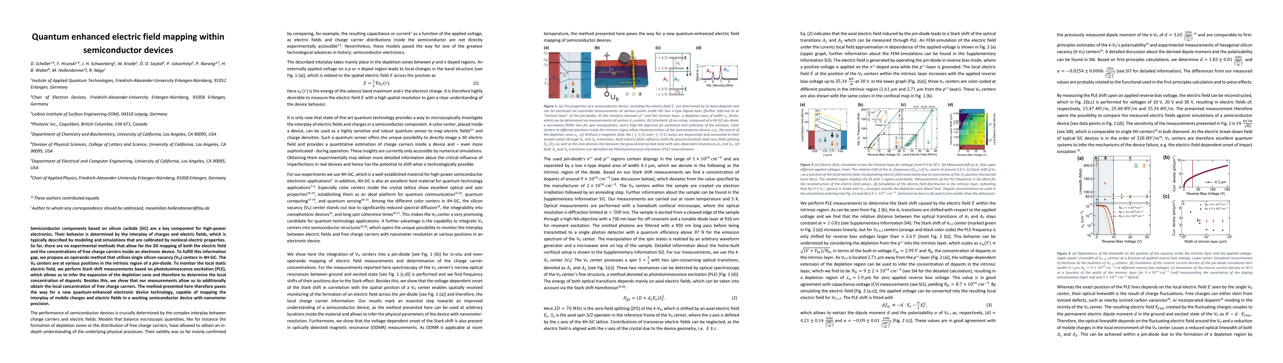
Semiconductor components based on silicon carbide (SiC) are a key component for high-power electronics. Their behavior is determined by the interplay of charges and electric fields, which is typically described by modeling and simulations that are calibrated by nonlocal electric properties. So far, there are no experimental methods that allow for the 3D mapping of both the electric field and the concentrations of free charge carriers inside an electronic device. To fulfill this information gap, we propose an operando method that utilizes single silicon vacancy (VSi) centers in 4H-SiC. The VSi centers are at various positions in the intrinsic region of a pin-diode. To monitor the local static electric field, we perform Stark shift measurements based on photoluminescence excitation (PLE), which allows us to infer the expansion of the depletion zone and therefore to determine the local concentration of dopants. Besides this, we show that our measurements allow us to additionally obtain the local concentration of free charge carriers. The method presented here therefore paves the way for a new quantum-enhanced electronic device technology, capable of mapping the interplay of mobile charges and electric fields in a working semiconductor device with nanometer precision.
AI Key Findings
Get AI-generated insights about this paper's methodology, results, significance, and more — seven facets brought into focus.
Impact
Authors
PDF Preview
Citation Network
Current paper (gray), citations (green), references (blue)
Display is limited for performance on very large graphs.
Discussion 0