The study employs molecular beam epitaxy (MBE) to fabricate optically active indium selenide crystal phase heterostructures, with growth conditions controlled by adjusting In/Se flux ratio and temperature. Characterization techniques include RHEED, Raman scattering, photoluminescence (PL), AFM, and STEM.
Publication
Metrics
Quick Answers
What methodology did the authors use?
The study employs molecular beam epitaxy (MBE) to fabricate optically active indium selenide crystal phase heterostructures, with growth conditions controlled by adjusting In/Se flux ratio and temperature. Characterization techniques include RHEED, Raman scattering, photoluminescence (PL), AFM, and STEM. More in Methodology →
What are the key results?
The γ-InSe/γ-In2Se3 heterostructure emits intense optical signals in the near-infrared range with tunable emission energy via quantum size effect. — Emission energy shifts by 250 meV as γ-InSe layer thickness decreases below 20 nm, attributed to quantum confinement. More in Key Results →
Why is this work significant?
This research provides a platform for designing near-infrared light sources and detectors using tunable optically active heterostructures, with potential applications in photonic devices. More in Significance →
What are the main limitations?
Optical emission from very thin γ-InSe layers becomes too weak for detection. — Substrate-related emissions limit spectral analysis in certain ranges. More in Limitations →
Abstract
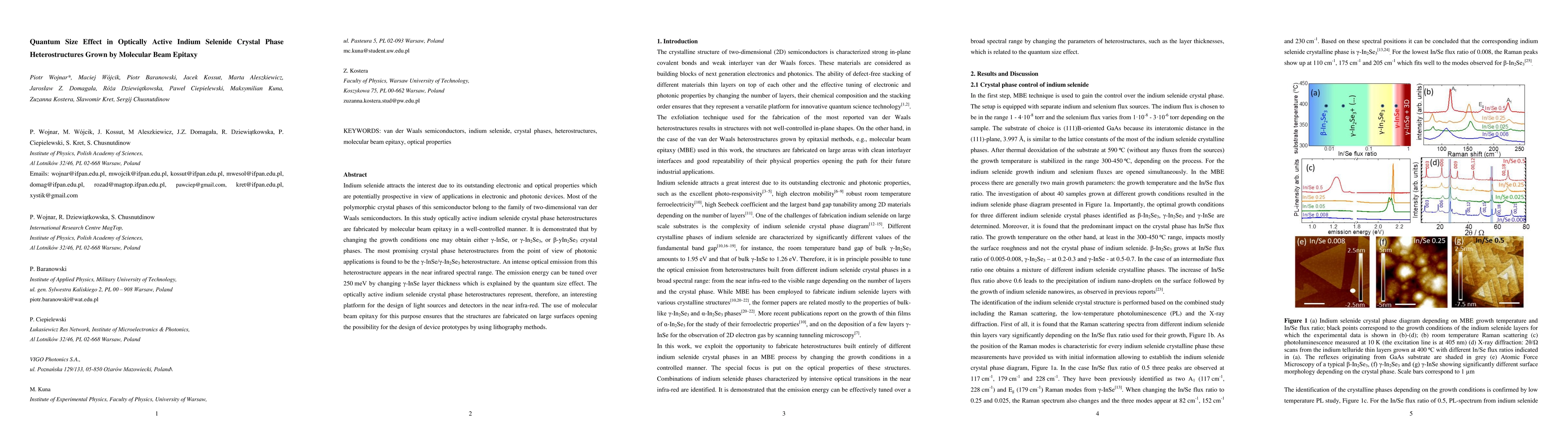
Indium selenide attracts the interest due to its outstanding electronic and optical properties which are potentially prospective in view of applications in electronic and photonic devices. Most of the polymorphic crystal phases of this semiconductor belong to the family of two-dimensional van der Waals semiconductors. In this study optically active indium selenide crystal phase heterostructures are fabricated by molecular beam epitaxy in a well-controlled manner. It is demonstrated that by changing the growth conditions one may obtain either {\gamma}-InSe, or {\gamma}-In2Se3, or \b{eta}-yIn2Se3 crystal phases. The most promising crystal phase heterostructures from the point of view of photonic applications is found to be the {\gamma}-InSe/{\gamma}-In2Se3 heterostructure. An intense optical emission from this heterostructure appears in the near infrared spectral range. The emission energy can be tuned over 250 meV by changing {\gamma}-InSe layer thickness which is explained by the quantum size effect. The optically active indium selenide crystal phase heterostructures represent, therefore, an interesting platform for the design of light sources and detectors in the near infra-red. The use of molecular beam epitaxy for this purpose ensures that the structures are fabricated on large surfaces opening the possibility for the design of device prototypes by using lithography methods
Key Findings, in focus
Seven facets of this paper, analysed and brought into focus by AI.
This research provides a platform for designing near-infrared light sources and detectors using tunable optically active heterostructures, with potential applications in photonic devices.
- The γ-InSe/γ-In2Se3 heterostructure emits intense optical signals in the near-infrared range with tunable emission energy via quantum size effect.
- Emission energy shifts by 250 meV as γ-InSe layer thickness decreases below 20 nm, attributed to quantum confinement.
- Staggered band alignment at the γ-InSe/γ-In2Se3 interface explains lower emission energy compared to bulk γ-InSe.
This research provides a platform for designing near-infrared light sources and detectors using tunable optically active heterostructures, with potential applications in photonic devices.
Demonstration of controlled MBE growth of multiple indium selenide crystal phases with sharp interfaces and characterization of their optoelectronic properties.
First demonstration of quantum size effect tuning in γ-InSe/γ-In2Se3 heterostructures for near-infrared emission, combined with precise phase control via MBE.
- Optical emission from very thin γ-InSe layers becomes too weak for detection.
- Substrate-related emissions limit spectral analysis in certain ranges.
- Exploring other crystal phase combinations for broader spectral tuning.
- Investigating device integration and scalability for practical applications.
Discussion 0