01
MethodologyHow they did it
Systematic investigation of first and second harmonic apparent piezoresponses in Si wafer using SPM techniques
This paper investigates the quadratic electromechanical strain in silicon using piezoresponse force microscopy, revealing a significant second harmonic response in vertical mode, likely due to ionic electrochemical dipoles. The study differentiates between true piezoelectricity and apparent responses, providing methods to distinguish them.
This paper investigates the quadratic electromechanical strain in silicon using piezoresponse force microscopy, revealing a significant second harmonic response in vertical mode, likely due to ionic electrochemical dipoles. The study differentiates between true piezoelectricity and apparent responses, providing methods to distinguish them.
Systematic investigation of first and second harmonic apparent piezoresponses in Si wafer using SPM techniques More in Methodology →
Si wafer exhibits apparent electromechanical response under a charged probe that may arise from induced electrochemical dipoles — The electromechanical response measured is dominated by the second harmonic quadratic response in vertical mode More in Key Results →
Understanding the origin of apparent piezoresponses in Si wafer is crucial for developing new nanoscale devices and sensors More in Significance →
Limited to a single type of material (Si) and measurement technique (SPM) — Potential artifacts from probe-induced damage or surface contamination More in Limitations →
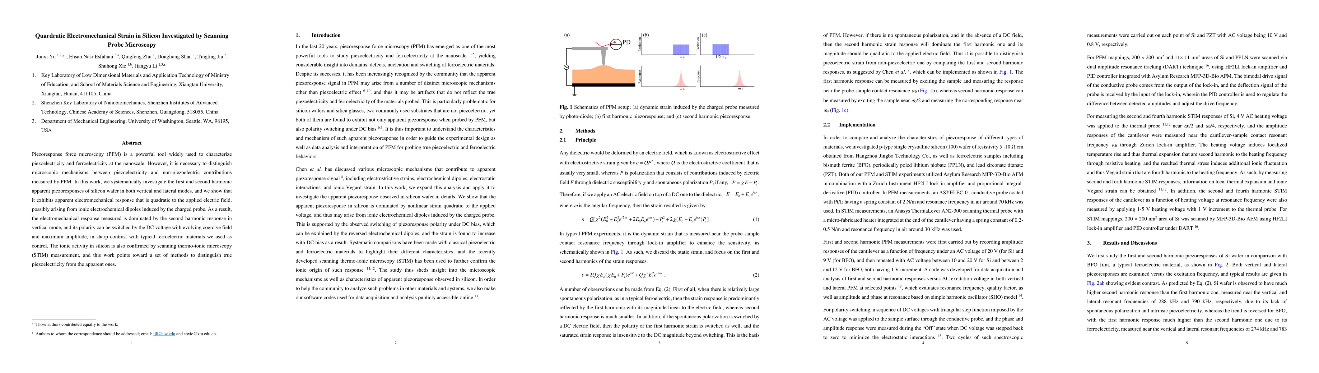
Piezoresponse force microscopy (PFM) is a powerful tool widely used to characterize piezoelectricity and ferroelectricity at the nanoscale. However, it is necessary to distinguish microscopic mechanisms between piezoelectricity and non-piezoelectric contributions measured by PFM. In this work, we systematically investigate the first and second harmonic apparent piezoresponses of silicon wafer in both vertical and lateral modes, and we show that it exhibits apparent electromechanical response that is quadratic to the applied electric field, possibly arising from ionic electrochemical dipoles induced by the charged probe. As a result, the electromechanical response measured is dominated by the second harmonic response in vertical mode, and its polarity can be switched by the DC voltage with evolving coercive field and maximum amplitude, in sharp contrast with typical ferroelectric materials we used as control. The ionic activity in silicon is also confirmed by scanning thermo-ionic microscopy (STIM) measurement, and this work points toward a set of methods to distinguish true piezoelectricity from the apparent ones.
Seven facets of this paper, analysed and brought into focus by AI.
Understanding the origin of apparent piezoresponses in Si wafer is crucial for developing new nanoscale devices and sensors
Systematic investigation of first and second harmonic apparent piezoresponses in Si wafer using SPM techniques
Understanding the origin of apparent piezoresponses in Si wafer is crucial for developing new nanoscale devices and sensors
Development of a novel understanding of the relationship between electrochemical dipoles and apparent piezoresponses in Si wafer
The work presents a new perspective on the origin of apparent piezoresponses in Si wafer, which has significant implications for nanoscale device development
Current paper (gray), citations (green), references (blue)
Display is limited for performance on very large graphs.
Discussion 0