The research employs micro-focused angle-resolved photoemission spectroscopy (µ-ARPES) to separate band gap renormalization effects in single-layer WS2 due to environmental screening and electron-doping during in situ gating. The WS2 is supported on hexagonal boron nitride (hBN) and has sections exposed to vacuum and encapsulated by a graphene contact.
Quasiparticle gap renormalization driven by internal and external screening in WS$_2$ device
Publication
Metrics
AI Quick Summary
This study investigates the quasiparticle gap renormalization in single-layer WS$_2$ using micro-focused angle resolved photoemission spectroscopy, revealing that intrinsic doping-induced screening in vacuum-exposed WS$_2$ surpasses the external environmental screening in graphene-encapsulated WS$_2$, leading to greater band gap renormalization.
Quick Answers
What is "Quasiparticle gap renormalization driven by internal and external screening in WS$_2$ device" about?
This study investigates the quasiparticle gap renormalization in single-layer WS$_2$ using micro-focused angle resolved photoemission spectroscopy, revealing that intrinsic doping-induced screening in vacuum-exposed WS$_2$ surpasses the external environmental screening in graphene-encapsulated WS$_2$, leading to greater band gap renormalization.
What methodology did the authors use?
The research employs micro-focused angle-resolved photoemission spectroscopy (µ-ARPES) to separate band gap renormalization effects in single-layer WS2 due to environmental screening and electron-doping during in situ gating. The WS2 is supported on hexagonal boron nitride (hBN) and has sections exposed to vacuum and encapsulated by a graphene contact. More in Methodology →
What are the key results?
Direct observation of a doping-induced semiconductor-metal transition and band gap renormalization in WS2 sections. — Larger band gap renormalization observed in the vacuum-exposed section compared to the graphene-encapsulated section, attributed to stronger intrinsic screening due to doping in the vacuum-exposed WS2. More in Key Results →
Why is this work significant?
This study provides insights into how the electronic band gap of 2D semiconductors is sensitive to variations in screening properties and gate-controlled doping, which is crucial for designing and optimizing device architectures. More in Significance →
What are the main limitations?
The research is limited to a specific device architecture involving WS2, hBN, and graphene. — The findings may not be universally applicable to all 2D semiconductor materials or device configurations. More in Limitations →
Abstract
The electronic band gap of a two-dimensional semiconductor within a device architecture is sensitive to variations in screening properties of adjacent materials in the device and to gate-controlled doping. Here, we employ micro-focused angle resolved photoemission spectroscopy to separate band gap renormalization effects stemming from environmental screening and electron-doping during \textit{in situ} gating of a single-layer WS$_{2}$ device. The WS$_{2}$ is supported on hBN and contains a section that is exposed to vacuum and another section that is encapsulated by a graphene contact. We directly observe the doping-induced semiconductor-metal transition and band gap renormalization in the two sections of WS$_2$. Surprisingly, a larger band gap renormalization is observed in the vacuum-exposed section than in the graphene-encapsulated - and thus ostensibly better screened - section of the WS$_2$. Using $GW$ calculations, we determine that intrinsic screening due to stronger doping in vacuum exposed WS$_2$ exceeds the external environmental screening in graphene-encapsulated WS$_2$.
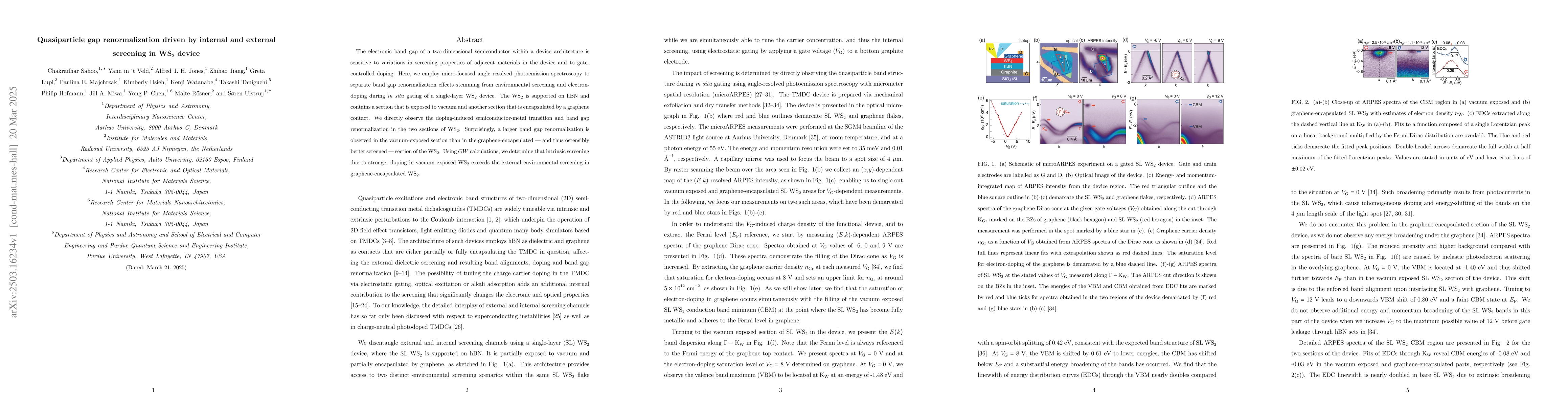
Key Findings, in focus
Seven facets of this paper, analysed and brought into focus by AI.
This study provides insights into how the electronic band gap of 2D semiconductors is sensitive to variations in screening properties and gate-controlled doping, which is crucial for designing and optimizing device architectures.
- Direct observation of a doping-induced semiconductor-metal transition and band gap renormalization in WS2 sections.
- Larger band gap renormalization observed in the vacuum-exposed section compared to the graphene-encapsulated section, attributed to stronger intrinsic screening due to doping in the vacuum-exposed WS2.
- GW calculations confirm that intrinsic screening in vacuum-exposed WS2 exceeds external environmental screening in graphene-encapsulated WS2.
This study provides insights into how the electronic band gap of 2D semiconductors is sensitive to variations in screening properties and gate-controlled doping, which is crucial for designing and optimizing device architectures.
The paper presents a detailed µ-ARPES study to disentangle the effects of environmental and doping-induced screening on band gap renormalization in WS2, supported by GW calculations.
The novelty lies in the direct observation and comparison of band gap renormalization in WS2 sections with distinct screening environments, revealing the dominant role of intrinsic doping-induced screening over external environmental screening.
- The research is limited to a specific device architecture involving WS2, hBN, and graphene.
- The findings may not be universally applicable to all 2D semiconductor materials or device configurations.
- Investigate similar effects in other 2D semiconductor materials to generalize the findings.
- Explore how different encapsulation materials or device geometries might influence screening and band gap renormalization.
Impact
Paper Details
Authors
PDF Preview
Citation Network
Current paper (gray), citations (green), references (blue)
Display is limited for performance on very large graphs.
Discussion 0