This paper presents a deep learning-based method using YOLO models to rapidly characterize 2D TMDs and lateral heterostructures, achieving over 94.67% accuracy. The approach also leverages transfer learning for enhanced performance and real-time analysis via an application, significantly improving efficiency and cost-effectiveness compared to traditional methods.
No key terms available for this paper.
Two-dimensional (2D) materials and heterostructures exhibit unique physical properties, necessitating efficient and accurate characterization methods. Leveraging advancements in artificial intelligence, we introduce a deep learning-based method for efficiently characterizing heterostructures and 2D materials, specifically MoS2-MoSe2 lateral heterostructures and MoS2 flakes with varying shapes and thicknesses. By utilizing YOLO models, we achieve an accuracy rate of over 94.67% in identifying these materials. Additionally, we explore the application of transfer learning across different materials, which further enhances model performance. This model exhibits robust generalization and anti-interference ability, ensuring reliable results in diverse scenarios. To facilitate practical use, we have developed an application that enables real-time analysis directly from optical microscope images, making the process significantly faster and more cost-effective than traditional methods. This deep learning-driven approach represents a promising tool for the rapid and accurate characterization of 2D materials, opening new avenues for research and development in material science.
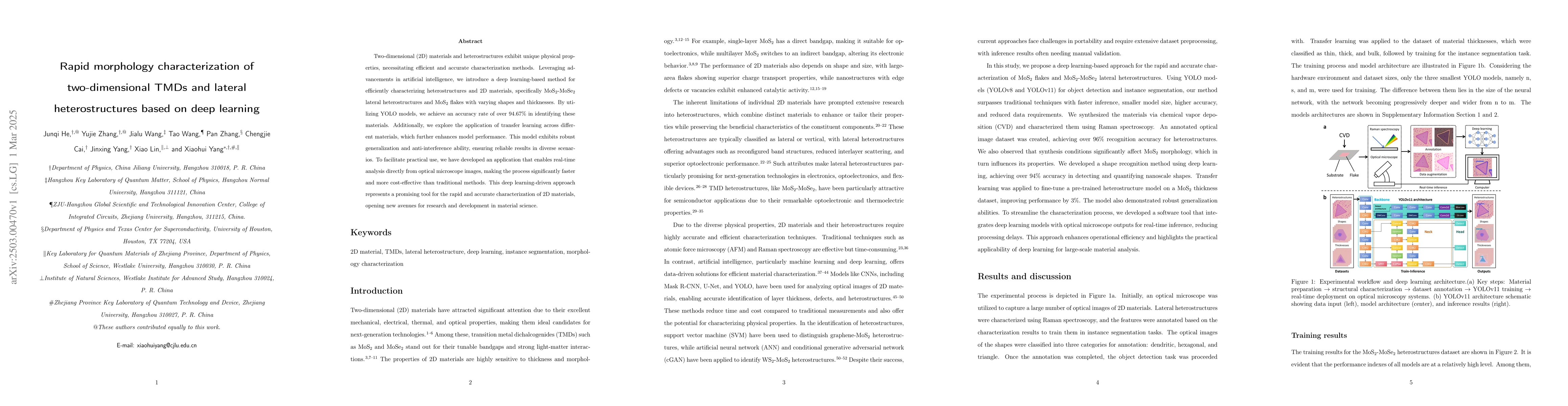
This graph shows how this paper is connected to other research. The current paper is shown in dark gray, papers that cite it are in green, and papers it references are in blue. You can:
• Hover over any node to see the paper title
• Click a node to view that paper's details
• Drag nodes to rearrange the graph
• Use the zoom controls (bottom right) to zoom in/out
No citations found for this paper.
Title | Authors | Year | Actions |
---|---|---|---|
Machine learning assisted fast optical identification of 2D materials
|
Junqi He, Yi Zhou, Pan Zhang, Huifei Zhai
|
2024
|
View Paper |
Interfacial thermal conductance in 2D WS2/MoSe2 and MoS2/MoSe2 lateral heterostructures
|
Shihao Xu, Peichen Wu, Youping Chen
|
2024
|
View Paper |
Identification and Structural Characterization of Twisted Atomically Thin Bilayer Materials by Deep Learning
|
Haitao Yang, Ruiqi Hu, Heng-Zhou Wu, Xiaolong He, Yan Zhou, Yizhe Xue, Kexin He, Wenshuai Hu, Haosen Chen, Min-Li Gong, Xin Zhang, Pingheng Tan, Eduardo R Hernández, Yong Xie
|
2024
|
View Paper |
When Machine Learning Meets 2D Materials: A Review
|
Bin Lu, Yuze Xia, Yuqian Ren, Miaomiao Xie, Liguo Zhou, G. Vinai, Simon A Morton, Andrew T S Wee, W. G. van der Wiel, Wen Zhang, P. Wong
|
2024
|
View Paper |
Controllable One-Pot Growth of MoSe2/WSe2 Lateral and Vertical Heterostructures by Facile Chemical Vapor Deposition
|
Xingyu Liu, Qianqian Wu, Mengde Dai, Qilei Xu, Xiumei Zhang, Zhengyang Cai, K. Ostrikov, Xiaofeng Gu, H. Nan, S. Xiao
|
2023
|
View Paper |
CVD graphene contacts for lateral heterostructure MoS2 field effect transistors
|
Daniel S. Schneider, L. Lucchesi, Eros Reato, Zhenyu Wang, Agata Piacentini, J. Bolten, D. Marian, E. G. Marín, A. Radenović, Zhenxing Wang, G. Fiori, A. Kis, G. Iannaccone, D. Neumaier, M. Lemme
|
2023
|
View Paper |
Review: 2D material property characterizations by machine-learning-assisted microscopies
|
Zhizhong Si, Daming Zhou, Jianlei Yang, Xiaoyang Lin
|
2023
|
View Paper |
Two-dimensional layered materials and heterostructures for flexible electronics
|
Anh Tuan Hoang, Luhing Hu, A. Katiyar, Jong-Hyun Ahn
|
2022
|
View Paper |
Deep‐Learning‐Based Microscopic Imagery Classification, Segmentation, and Detection for the Identification of 2D Semiconductors
|
Xingchen Dong, Hongwei Li, Yuntian Yan, Haoran Cheng, Hui Zhang, Yucheng Zhang, Tien Dat Le, Kun Wang, Jie Dong, M. Jakobi, A. Yetisen, A. Koch
|
2022
|
View Paper |
Understanding, discovery, and synthesis of 2D materials enabled by machine learning.
|
B. Ryu, Luqing Wang, H. Pu, M. Chan, Junhong Chen
|
2022
|
View Paper |
Artificial Neuron Networks Enabled Identification and Characterizations of 2D Materials and van der Waals Heterostructures.
|
Li Zhu, Jing Tang, Baichang Li, Tianyu Hou, Yong Zhu, Jiadong Zhou, Zhi Wang, Xiaorong Zhu, Zhenpeng Yao, Xu Cui, Kenji Watanabe, T. Taniguchi, Yafei Li, Z. Han, Wu Zhou, Yuang Huang, Zheng Liu, J. Hone, Yufeng Hao
|
2022
|
View Paper |
Uncovering material deformations via machine learning combined with four-dimensional scanning transmission electron microscopy
|
Chuqiao Shi, Michael C. Cao, Sarah M. Rehn, Sang-Hoon Bae, Jeehwan Kim, Matthew Jones, D. Muller, Yimo Han
|
2021
|
View Paper |
Recent advances and applications of deep learning methods in materials science
|
K. Choudhary, Brian L. DeCost, Chi Chen, Anubhav Jain, F. Tavazza, R. Cohn, Cheol Woo Park, A. Choudhary, Ankit Agrawal, S. Billinge, Elizabeth A. Holm, S. Ong, C. Wolverton
|
2021
|
View Paper |
The More, the Better–Recent Advances in Construction of 2D Multi‐Heterostructures
|
Ruijie Zhang, Menghan Li, Lin Li, Zhongming Wei, Fei Jiao, Dechao Geng, Wenping Hu
|
2021
|
View Paper |
3D Deep Learning Enables Accurate Layer Mapping of 2D Materials.
|
Xingchen Dong, Hongwei Li, Zhutong Jiang, Theresa Grünleitner, İnci Güler, Jie Dong, Kun Wang, Michael H. Köhler, M. Jakobi, Bjoern H Menze, A. Yetisen, I. Sharp, A. Stier, J. Finley, A. Koch
|
2021
|
View Paper |
Chemical Vapor Deposition Growth of Two-Dimensional Compound Materials: Controllability, Material Quality, and Growth Mechanism
|
Lei Tang, Junyang Tan, Huiyun Nong, Bilu Liu, Hui‐Ming Cheng
|
2020
|
View Paper |
Large Single‐Crystal Cu Foils with High‐Index Facets by Strain‐Engineered Anomalous Grain Growth
|
Yanglizhi Li, Luzhao Sun, Zhenghua Chang, Haiyang Liu, Yuechen Wang, Yu-Lun Liang, Buhang Chen, Qingjie Ding, Zhen Zhao, Ruoyu Wang, Yujie Wei, H. Peng, Li Lin, Zhongfan Liu
|
2020
|
View Paper |
Automated identification and characterization of two-dimensional materials via machine learning-based processing of optical microscope images
|
Juntan Yang, H. Yao
|
2020
|
View Paper |
Research status of MoSe2 and its composites: A review
|
X. Wu, Yu-hua Wang, Pei-ling Li, Zu-Zhao Xiong
|
2020
|
View Paper |
Excellent thermoelectric performance induced by interface effect in MoS2/MoSe2 van der Waals heterostructure
|
Pin-Zhen Jia, Yunling Zeng, Dan Wu, Huixin Pan, Xuan-Hao Cao, Wu-Xing Zhou, Zhong-Xiang Xie, Ji-Xu Zhang, Keqiu Chen
|
2019
|
View Paper |
Deep-learning-based image segmentation integrated with optical microscopy for automatically searching for two-dimensional materials
|
S. Masubuchi, Eisuke Watanabe, Yu-Seong Seo, S. Okazaki, T. Sasagawa, Kenji Watanabe, T. Taniguchi, T. Machida
|
2019
|
View Paper |
Borophene-graphene heterostructures
|
Xiaolong Liu, M. Hersam
|
2019
|
View Paper |
Rapid identification of two-dimensional materials via machine learning assisted optic microscopy
|
Yu-hao Li, Yangyang Kong, Jinlin Peng, Chuanbin Yu, Zhi Li, Penghui Li, Yunya Liu, C. Gao, Rong Wu
|
2019
|
View Paper |
Lateral and Vertical MoSe2-MoS2 Heterostructures via Epitaxial Growth: Triggered by High Temperature Annealing and Precursor Concentration.
|
Tao Chen, Degong Ding, Jia Shi, Guang Wang, Liangzhi Kou, Xiaoming Zheng, Xibiao Ren, Xinfeng Liu, C. Jin, J. Zhong, G. Hao
|
2019
|
View Paper |
The electronic thickness of graphene
|
P. Rickhaus, Ming-Hao Liu, M. Kurpas, A. Kurzmann, Yongjin Lee, H. Overweg, M. Eich, Riccardo Pisoni, T. Taniguchi, Kenji Watanabe, K. Richter, K. Ensslin, T. Ihn
|
2019
|
View Paper |
Classifying optical microscope images of exfoliated graphene flakes by data-driven machine learning
|
S. Masubuchi, T. Machida
|
2019
|
View Paper |
Scalable high performance radio frequency electronics based on large domain bilayer MoS2
|
Qingguo Gao, Zhenfeng Zhang, Xiaole Xu, Jian Song, Xuefei Li, Yanqing Wu
|
2018
|
View Paper |
Solution-processable 2D semiconductors for high-performance large-area electronics
|
Zhaoyang Lin, Yuan Liu, Udayabagya Halim, Mengning Ding, Yuanyue Liu, Yiliu Wang, Chuancheng Jia, Peng Chen, Xidong Duan, Chen Wang, F. Song, Mufang Li, Chengzhang Wan, Yu Huang, X. Duan
|
2018
|
View Paper |
Synthesis of transition metal dichalcogenides and their heterostructures
|
Yuhang Cai, Kai Xu, Wenjuan Zhu
|
2018
|
View Paper |
Interface Characterization and Control of 2D Materials and Heterostructures
|
Xiaolong Liu, M. Hersam
|
2018
|
View Paper |
Photocarrier Transfer across Monolayer MoS2-MoSe2 Lateral Heterojunctions.
|
Matthew Z. Bellus, M. Mahjouri‐Samani, Samuel D. Lane, Akinola D Oyedele, Xufan Li, A. Puretzky, D. Geohegan, Kai Xiao, Hui Zhao
|
2018
|
View Paper |
Intelligent identification of two-dimensional nanostructures by machine-learning optical microscopy
|
Xiaoyang Lin, Zhizhong Si, Wenzhi Fu, Jianlei Yang, S. Guo, Yuan Cao, Jin Zhang, Xinhe Wang, Peng Liu, K. Jiang, Weisheng Zhao
|
2018
|
View Paper |
Exploring Two-Dimensional Materials toward the Next-Generation Circuits: From Monomer Design to Assembly Control.
|
Mengqi Zeng, Yao Xiao, Jinxin Liu, Kena Yang, L. Fu
|
2018
|
View Paper |
NaCl-assisted one-step growth of MoS2–WS2 in-plane heterostructures
|
Zhan Wang, Yong Xie, Haolin Wang, Ruixue Wu, Tang Nan, Y. Zhan, Jing Sun, Teng Jiang, Ying Zhao, Yimin Lei, Mei Yang, Weidong Wang, Q. Zhu, Xiao-hua Ma, Y. Hao
|
2017
|
View Paper |
Direct Growth of High Mobility and Low-Noise Lateral MoS2 -Graphene Heterostructure Electronics.
|
A. Behranginia, P. Yasaei, A. Majee, V. Sangwan, Fei Long, C. Foss, Tara Foroozan, Shadi Fuladi, M. Hantehzadeh, R. Shahbazian‐Yassar, M. Hersam, Z. Akšamija, A. Salehi‐khojin
|
2017
|
View Paper |
In-Plane Mosaic Potential Growth of Large-Area 2D Layered Semiconductors MoS2-MoSe2 Lateral Heterostructures and Photodetector Application.
|
Xiaoshuang Chen, Yunfeng Qiu, Huihui Yang, Guangbo Liu, Wei Zheng, W. Feng, W. Cao, Wenping Hu, P. Hu
|
2017
|
View Paper |
Defects Engineered Monolayer MoS2 for Improved Hydrogen Evolution Reaction.
|
Gonglan Ye, Y. Gong, Junhao Lin, Bo Li, Yongmin He, S. Pantelides, Wu Zhou, R. Vajtai, P. Ajayan
|
2016
|
View Paper |
Recent development in 2D materials beyond graphene
|
Ankur Gupta, T. Sakthivel, S. Seal
|
2015
|
View Paper |
Role of Chemical Potential in Flake Shape and Edge Properties of Monolayer MoS2
|
D. Cao, Tao Shen, P. Liang, Xiaoshuang Chen, H. Shu
|
2015
|
View Paper |
Lateral epitaxial growth of two-dimensional layered semiconductor heterojunctions.
|
Xidong Duan, Chen Wang, J. Shaw, Rui Cheng, Yu Chen, Honglai Li, Xueping Wu, Ying Tang, Qinling Zhang, A. Pan, Jianhui Jiang, R. Yu, Yu Huang, X. Duan
|
2014
|
View Paper |
Shape Evolution of Monolayer MoS2 Crystals Grown by Chemical Vapor Deposition
|
Shanshan Wang, Youmin Rong, Ye Fan, M. Pacios, H. Bhaskaran, Kuang He, J. Warner
|
2014
|
View Paper |
Dendritic, transferable, strictly monolayer MoS2 flakes synthesized on SrTiO3 single crystals for efficient electrocatalytic applications.
|
Y. Zhang, Qingqing Ji, Gao-Feng Han, J. Ju, Jianping Shi, D. Ma, Jingyu Sun, Yanshuo Zhang, Minjie Li, X. Lang, Yanfeng Zhang, Zhongfan Liu
|
2014
|
View Paper |
First-principles Raman spectra of MoS2, WS2 and their heterostructures.
|
2014
|
View Paper | |
Few-layer MoS2: a promising layered semiconductor.
|
R. Ganatra, Qing Zhang
|
2014
|
View Paper |
Direct observation of the transition from indirect to direct bandgap in atomically thin epitaxial MoSe2.
|
Yi Zhang, Tay-Rong Chang, Bo Zhou, Yong-Tao Cui, Hao Yan, Zhongkai Liu, F. Schmitt, James J Lee, R. Moore, Yulin Chen, Hsin Lin, H. Jeng, S. Mo, Z. Hussain, A. Bansil, Z. Shen
|
2014
|
View Paper |
The chemistry of two-dimensional layered transition metal dichalcogenide nanosheets.
|
M. Chhowalla, H. Shin, G. Eda, Lain‐Jong Li, K. Loh, Hua Zhang
|
2013
|
View Paper |
2D materials: to graphene and beyond.
|
R. Mas‐Ballesté, C. Gómez-Navarro, J. Gómez‐Herrero, F. Zamora
|
2011
|
View Paper |
Identification of Active Edge Sites for Electrochemical H2 Evolution from MoS2 Nanocatalysts
|
T. Jaramillo, K. Jørgensen, J. Bonde, J. H. Nielsen, S. Horch, I. Chorkendorff
|
2007
|
View Paper |
Two-dimensional atomic crystals.
|
K. Novoselov, D. Jiang, F. Schedin, T. Booth, V. Khotkevich, S. Morozov, A.K. Geim
|
2005
|
View Paper |
Electric Field Effect in Atomically Thin Carbon Films
|
K. Novoselov, A.K. Geim, S. Morozov, D. Jiang, Y. Zhang, S. Dubonos, I. Grigorieva, A. Firsov
|
2004
|
View Paper |
Quantitative analysis of MoS 2 thin film micrographs with machine learning
|
2024
|
||
Size and shape control of CVD-grown monolayer MoS 2
|
2023
|
||
2D MoS 2-MoSe 2and MoS 2-NbS 2 Lateral Hetero Structures as Anode Materials for LIBs/SIBs
|
Gayatree Barik, S. Pal
|
2021
|
View Paper |
Waals contacts between three-dimensional metals and two-dimensional semiconductors
|
2019
|
||
Waals integration before and beyond two-dimensional materials
|
2019
|
||
Molybdenum diselenide (MoSe 2 ) for energy storage, catalysis, and opto-electronics
|
2017
|
||
Two-dimensional MoS 2 : Properties, preparation, and applications
|
2015
|
||
Deep learning-based multi-modal analysis for transition-metal dichalcogenides
|
Showing first page preview. Click "Open Full PDF" to view the complete paper.
Feng Zhang, Zheng Liu, Takashi Taniguchi, Kenji Watanabe, Susumu Okada, Mina Maruyama, Ryo Kitaura, Takato Hotta, Nanami Ichinose, Ruben Canton-Vitoria, Fanyu Zeng
Published: 2022-10-05
You need to log in to post a comment.
Your comment contains inappropriate language.
Are you sure you want to remove this tag?
Someone just favorited a paper!
Comments (0)