This paper reports the real-space mapping of electronic orbitals in bulk rutile (TiO2) using electron energy-loss spectrometry (EELS), revealing atomic-scale interactions. This technique enables experimental verification of theoretical predictions and opens new avenues for studying electronic states at defects and interfaces.
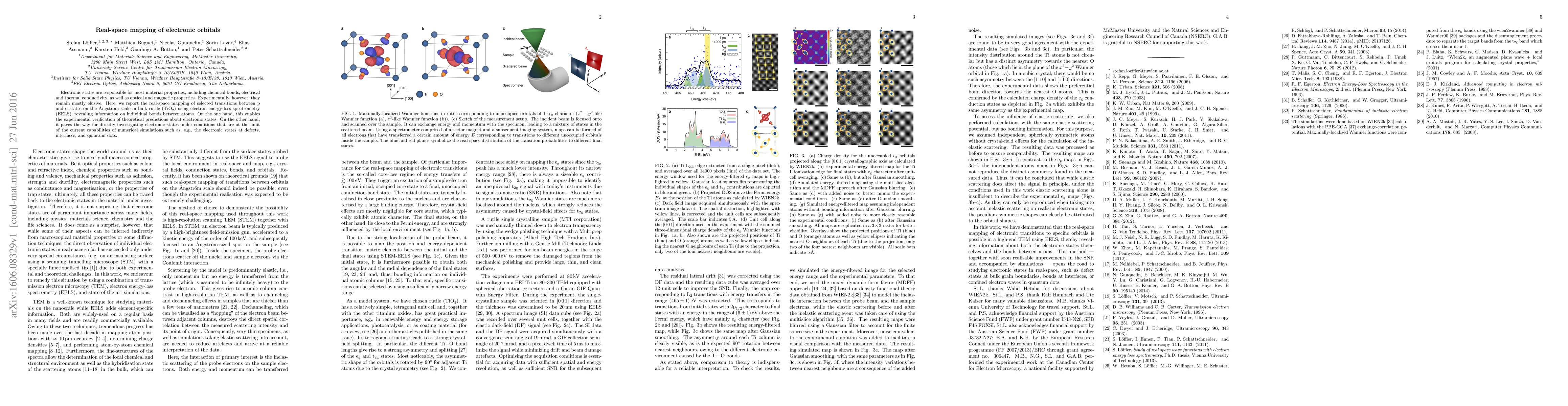
Electronic states are responsible for most material properties, including chemical bonds, electrical and thermal conductivity, as well as optical and magnetic properties. Experimentally, however, they remain mostly elusive. Here, we report the real-space mapping of selected transitions between p and d states on the {\AA}ngstr\"om scale in bulk rutile (TiO2) using electron energy-loss spectrometry (EELS), revealing information on individual bonds between atoms. On the one hand, this enables the experimental verification of theoretical predictions about electronic states. On the other hand, it paves the way for directly investigating electronic states under conditions that are at the limit of the current capabilities of numerical simulations such as, e.g., the electronic states at defects, interfaces, and quantum dots.
Get AI-generated insights about this paper's methodology, results, and significance.
Current paper (gray), citations (green), references (blue)
Edward F. Valeev, Robert J. Harrison. Adam A. Holmes, Charles C. Peterson et al.
L. Li, D. M. Kepaptsoglou, Q. M. Ramasse et al.
Title | Authors | Year | Actions |
---|---|---|---|
Low-voltage single-atom electron microscopy with carbon-based nanomaterials.
|
Aowen Li, Ang Li, Wu Zhou
|
2024
|
View Paper |
Current opinion on the prospect of mapping electronic orbitals in the transmission electron microscope: State of the art, challenges and perspectives.
|
M. Bugnet, S. Löffler, M. Ederer, D. Kepaptsoglou, Q. Ramasse
|
2024
|
View Paper |
Direct imaging of electron density with a scanning transmission electron microscope
|
Ondrej Dyck, Jawaher Almutlaq, D. Lingerfelt, Jacob L Swett, M. Oxley, Bevin Huang, A. Lupini, Dirk Englund, Stephen Jesse
|
2023
|
View Paper |
Probing a Defect-Site-Specific Electronic Orbital in Graphene with Single-Atom Sensitivity.
|
Mingquan Xu, Aowen Li, S. J. Pennycook, Shangpeng Gao, Wu Zhou
|
2023
|
View Paper |
Visualising emergent phenomena at oxide interfaces
|
Michael Oberaigner, M. Ederer, S. Chaluvadi, P. Orgiani, R. Ciancio, Stefan Loffler, Gerald Kothleitner, Daniel Knez
|
2023
|
View Paper |
4D Energy-Filtered STEM: A New Approach for Mapping Orbital Transitions.
|
S. Löffler, M. Ederer
|
2023
|
View Paper |
Four-dimensional electron energy-loss spectroscopy.
|
Mei Wu, R. Shi, Ruishi Qi, Yuehui Li, Jinlong Du, Peng Gao
|
2023
|
View Paper |
Optimizing experimental parameters for orbital mapping.
|
M. Ederer, S. Löffler
|
2023
|
View Paper |
Different atomic contrasts in HAADF images and EELS maps of rutile TiO2.
|
C. Iwashimizu, M. Haruta, T. Nemoto, H. Kurata
|
2022
|
View Paper |
Electron orbital mapping of SrTiO3 using electron energy-loss spectroscopy
|
C. Iwashimizu, M. Haruta, H. Kurata
|
2021
|
View Paper |
Image difference metrics for high-resolution electron microscopy.
|
M. Ederer, S. Löffler
|
2021
|
View Paper |
Imaging the Spatial Distribution of Electronic States in Graphene Using Electron Energy-Loss Spectroscopy: Prospect of Orbital Mapping.
|
M. Bugnet, M. Ederer, V. Lazarov, L. Li, Q. Ramasse, S. Löffler, D. Kepaptsoglou
|
2021
|
View Paper |
Exploiting the Acceleration Voltage Dependence of EMCD
|
S. Löffler, M. Stöger-Pollach, A. Steiger-Thirsfeld, W. Hetaba, P. Schattschneider
|
2021
|
View Paper |
Bridging nano-optics and condensed matter formalisms in a unified description of inelastic scattering of relativistic electron beams
|
H. Lourencco-Martins, A. Lubk, M. Kociak
|
2020
|
View Paper |
Two-dimensional electron systems in perovskite oxide heterostructures: Role of the polarity-induced substitutional defects
|
Shih-Chieh Lin, C. Kuo, Y. Shao, Y. Chuang, J. Geessinck, M. Huijben, J. Rueff, I. L. Graff, G. Conti, Y. Peng, A. Bostwick, E. Rotenberg, E. Gullikson, S. Nemšák, A. Vailionis, N. Gauquelin, J. Verbeeck, G. Ghiringhelli, C. Schneider, C. Fadley
|
2019
|
View Paper |
Growth Control and Thickness Measurement of Thin Films
|
C. Eisenmenger-Sittner
|
2019
|
View Paper |
Direct Detection Electron Energy-Loss Spectroscopy: A Method to Push the Limits of Resolution and Sensitivity
|
J. Hart, A. Lang, A. Leff, P. Longo, C. Trevor, R. Twesten, M. Taheri
|
2017
|
View Paper |
Measurement of atomic electric fields and charge densities from average momentum transfers using scanning transmission electron microscopy.
|
K. Müller-Caspary, F. Krause, T. Grieb, S. Löffler, M. Schowalter, A. Béché, Vincent Galioit, Dennis Marquardt, J. Zweck, P. Schattschneider, J. Verbeeck, A. Rosenauer
|
2017
|
View Paper |
Analytical Electron Microscopy
|
G. Botton, S. Prabhudev
|
2019
|
View Paper |
Comments (0)