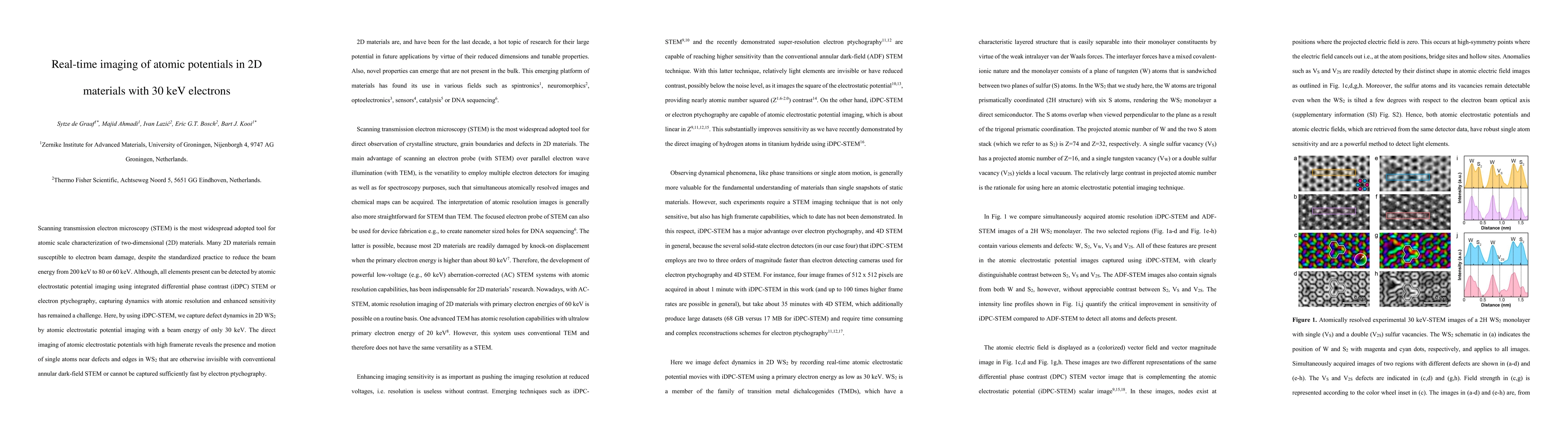
Publication
Metrics
AI Quick Summary
This paper demonstrates the use of integrated differential phase contrast (iDPC) scanning transmission electron microscopy (STEM) at 30 keV to capture atomic electrostatic potentials in 2D materials, revealing defect dynamics in WS$_2$ with high resolution and sensitivity, overcoming limitations of conventional STEM and electron ptychography.
Paper Preview
Abstract
Scanning transmission electron microscopy (STEM) is the most widespread adopted tool for atomic scale characterization of two-dimensional (2D) materials. Many 2D materials remain susceptible to electron beam damage, despite the standardized practice to reduce the beam energy from 200 keV to 80 or 60 keV. Although, all elements present can be detected by atomic electrostatic potential imaging using integrated differential phase contrast (iDPC) STEM or electron ptychography, capturing dynamics with atomic resolution and enhanced sensitivity has remained a challenge. Here, by using iDPC-STEM, we capture defect dynamics in 2D WS$_2$ by atomic electrostatic potential imaging with a beam energy of only 30 keV. The direct imaging of atomic electrostatic potentials with high framerate reveals the presence and motion of single atoms near defects and edges in WS$_2$ that are otherwise invisible with conventional annular dark-field STEM or cannot be captured sufficiently fast by electron ptychography.
AI Key Findings
Get AI-generated insights about this paper's methodology, results, significance, and more — seven facets brought into focus.
Impact
Paper Details
Authors
PDF Preview
Key Terms
Citation Network
Current paper (gray), citations (green), references (blue)
Display is limited for performance on very large graphs.
Discussion 0