Authors
Summary
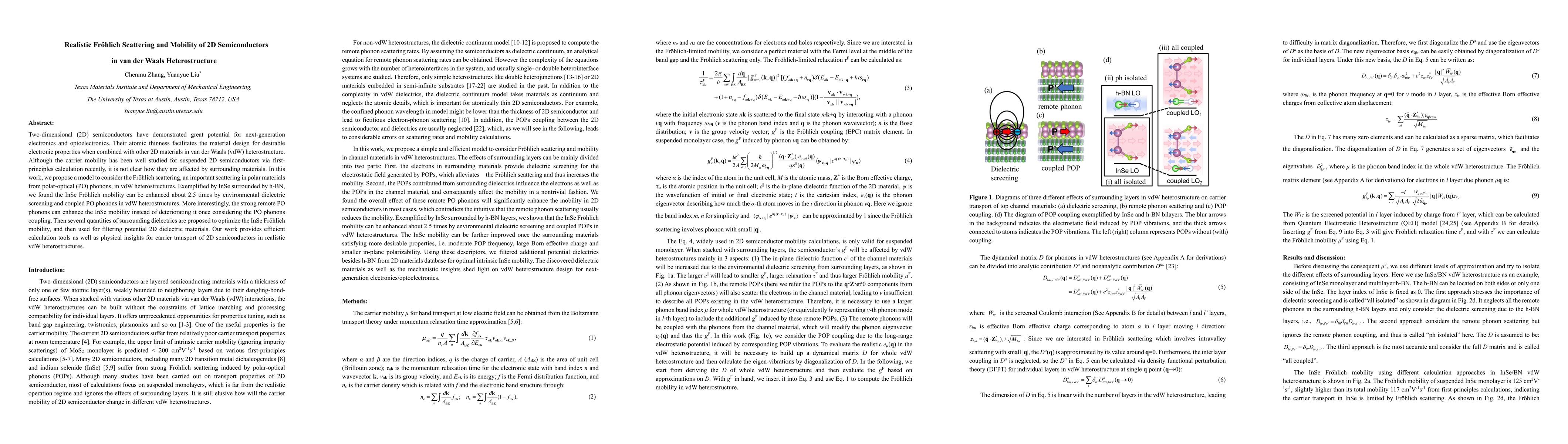
Two-dimensional (2D) semiconductors have demonstrated great potential for next-generation electronics and optoelectronics. Their atomic thinness facilitates the material design for desirable electronic properties when combined with other 2D materials in van der Waals (vdW) heterostructure. Although the carrier mobility has been well studied for suspended 2D semiconductors via first-principles calculation recently, it is not clear how they are affected by surrounding materials. In this work, we propose a model to consider the Fr\"ohlich scattering, an important scattering in polar materials from polar-optical (PO) phonons, in vdW heterostructures. Exemplified by InSe surrounded by h-BN, we found the InSe Fr\"ohlich mobility can be enhanced about 2.5 times by environmental dielectric screening and coupled PO phonons in vdW heterostructures. More interestingly, the strong remote PO phonons can enhance the InSe mobility instead of deteriorating it once considering the PO phonons coupling. Then several quantities of surrounding dielectrics are proposed to optimize the InSe Fr\"ohlich mobility, and then used for filtering potential 2D dielectric materials. Our work provides efficient calculation tools as well as physical insights for carrier transport of 2D semiconductors in realistic vdW heterostructures.
AI Key Findings
Get AI-generated insights about this paper's methodology, results, and significance.
Paper Details
PDF Preview
Key Terms
Similar Papers
Found 4 papersObservation of Photoluminescence from a Natural van der Waals Heterostructure
K. Watanabe, Viviane Z. Costa, Bryce Baker et al.
No citations found for this paper.
Comments (0)