ArxivLens

Quick Summary:

This paper reviews recent advancements in the synthesis and applications of heterostructures combining two-dimensional materials with wide bandgap semiconductors, highlighting their potential to enhance electronic and optoelectronic devices. It discusses construction methods, diverse applications, and future research directions.

DOI: 10.1088/1361-648X/ac5310
arXiv Id: 2203.03895
Date Published: 2022-04-12
Date Updated: 2022-04-12

Key Terms (TF-IDF):

materials (0.265)
devices (0.257)
materials (0.256)
devices (0.244)
progress (0.177)
progress (0.175)
applications (0.175)
electronic (0.170)
applications (0.166)
electronic (0.159)
layer (0.155)
layer (0.153)
high (0.150)
high (0.145)
thermal conductivity (0.134)
high frequency (0.132)
prospects (0.131)
semiconductors (0.131)
micro (0.130)
foundation (0.130)
License: http://creativecommons.org/licenses/by-nc-nd/4.0/

Summary:

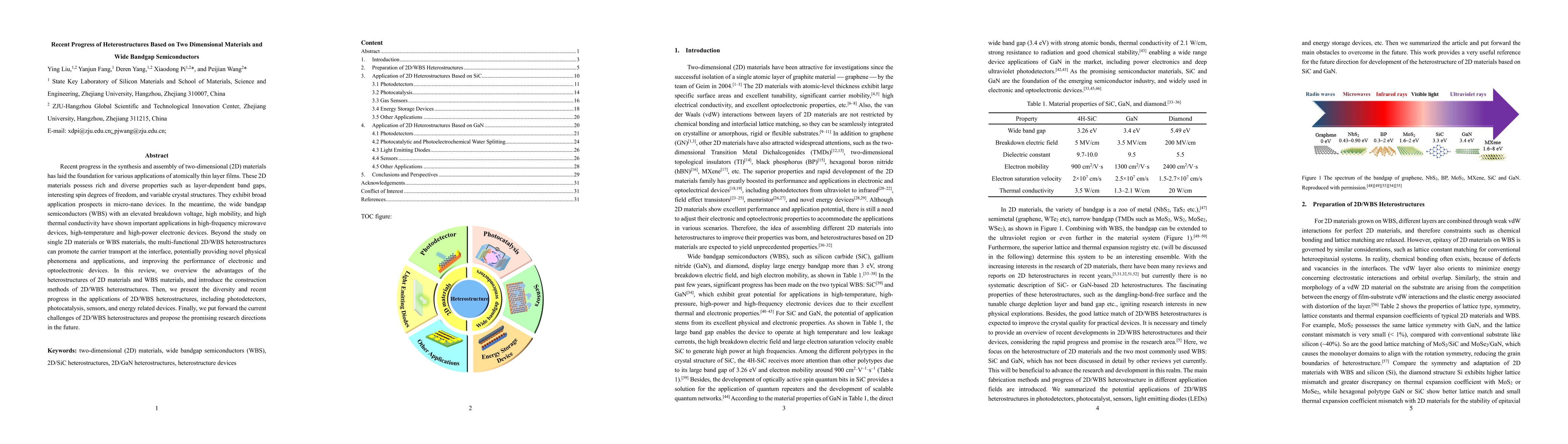
Recent progress in the synthesis and assembly of two-dimensional (2D) materials has laid the foundation for various applications of atomically thin layer films. These 2D materials possess rich and diverse properties such as layer-dependent band gaps, interesting spin degrees of freedom, and variable crystal structures. They exhibit broad application prospects in micro-nano devices. In the meantime, the wide bandgap semiconductors (WBS) with an elevated breakdown voltage, high mobility, and high thermal conductivity have shown important applications in high-frequency microwave devices, high-temperature and high-power electronic devices. Beyond the study on single 2D materials or WBS materials, the multi-functional 2D/WBS heterostructures can promote the carrier transport at the interface, potentially providing novel physical phenomena and applications, and improving the performance of electronic and optoelectronic devices. In this review, we overview the advantages of the heterostructures of 2D materials and WBS materials, and introduce the construction methods of 2D/WBS heterostructures. Then, we present the diversity and recent progress in the applications of 2D/WBS heterostructures, including photodetectors, photocatalysis, sensors, and energy related devices. Finally, we put forward the current challenges of 2D/WBS heterostructures and propose the promising research directions in the future.

Citation & Reference Network Visualization

This graph shows how this paper is connected to other research. The current paper is shown in dark gray, papers that cite it are in green, and papers it references are in blue. You can:

Current Paper
Papers citing this work (Citations)
Papers cited by this work (References)

• Hover over any node to see the paper title

• Click a node to view that paper's details

• Drag nodes to rearrange the graph

• Use the zoom controls (bottom right) to zoom in/out

Citations and References

Title Authors Year Actions
Quasi-2D material based heterostructure devices and its applications
V. Gautam, S. Verma, Roshani Singh, Zaid Ashraf, Kavindra Kandpal, Pramod Kumar
2024
View Paper
Modeling the Impact of AlGaAs Heterostructure Barrier Layer Thickness on Microwave Characteristics of Transistors Based on 0.15 μm pHEMT LNA Technology
Alexandr E. Shesterikov, Darya A. Shesterikova, Evgeniy V. Erofeev
2024
View Paper
Recent Advances in Layered MX2-Based Materials (M = Mo, W and X = S, Se, Te) for Emerging Optoelectronic and Photo(electro)catalytic Applications
Felipe M. Pinto, Mary C. M. D. de Conti, Wyllamanney S. Pereira, Júlio C. Sczancoski, Marina Medina, P. Corradini, J. F. de Brito, André E. Nogueira, Márcio S. Góes, Odair P. Ferreira, L. Mascaro, Fernando Wypych, F. A. L. La Porta
2024
View Paper
Carbon-contaminated topological defects in hexagonal boron nitride for quantum photonics
Rohit Babar, 'Ad'am Ganyecz, I. Abrikosov, Gergely Barcza, Viktor Iv'ady
2024
View Paper
Thinner 2D α-MoO3 makes setting up memristors easier
Yukun Hong, Shangui Lan, Baojun Pan, Zhixiang Zhang, Bingbing Chen, Lijie Zhang, Peijian Wang
2024
View Paper
Interface Properties of MoS2 van der Waals Heterojunctions with GaN
S. Panasci, I. Deretzis, E. Schilirò, A. La Magna, F. Roccaforte, A. Koos, Miklós Németh, B. Pécz, M. Cannas, S. Agnello, F. Giannazzo
2024
View Paper
Electrically Erasable Wide-Bandgap Charge-Trap Memory With an Electric-Flux-Modulating Counter Electrode
Hayoung Kim, A. Boampong, Chang-Hyun Kim, Min-Hoi Kim
2023
View Paper
Modeling and formation of a single-walled carbon nanotube (SWCNT) based heterostructure for efficient solar energy: Performance and defect analysis by numerical simulation
Md Ariful Islam, Jobair Al Rafi, Muhammad Athar Uddin
2023
View Paper
A carbon microsphere-modified ZnS-MnS@C composite anode for Li-ion battery applications
P. Naveenkumar, Munisamy Maniyazagan, Nayoung Kang, Hyeon-Woo Yang, W. Kang, Sun-Jae Kim
2023
View Paper
Electron Correlation in 2D Periodic Systems from Periodic Bootstrap Embedding.
O. R. Meitei, T. Van Voorhis
2023
View Paper
Integrating 2D layered materials with 3D bulk materials as van der Waals heterostructures for photodetections: Current status and perspectives
Weijie Liu, Yiye Yu, Meng Peng, Zhihua Zheng, Pengcheng Jian, Yang Wang, Yuanchen Zou, Yongming Zhao, Fang Wang, Feng Wu, Changqin Chen, J. Dai, Peng Wang, Weida Hu
2023
View Paper
Mechanochemical grinding diamond film using titanium-coated diamond active abrasives prepared by vacuum micro-evaporation coating
Yingke Zhou, J. Zang, Shengyao Su, Chaoyang Zhang, Lixiang Zhao, Yungang Yuan, Yanhui Wang, Jing Lu, Xipeng Xu, Pingwei Zhang
2023
View Paper
Optimized dopant imaging for GaN by a scanning electron microscopy
Kai Zhang, Chun‐guang Ban, Ye Yuan, Li Huang
2023
View Paper
Fast Response and High-Performance UV-C to NIR Broadband Photodetector based on MoS2/a-Ga2O3 heterostructures and impact of Band-alignment and Charge Carrier Dynamics
Riya Wadhwa, Damanpreet Kaur, Yuchen Zhang, Akhil Alexender, Deepu Kumar, Pradeep Kumar, Manoj A G Namboothiry, Quinn Qiao, Mukesh Kumar
2023
View Paper
High-performance flexible broadband photodetectors enabled by 2D Ta2NiSe5 nanosheets
Tingting Guo, Zixu Sa, Pengfei Wei, Yuxuan Jian, Xiang Chen, Zhesheng Chen, J. Avila, P. Dudin, Zai‐xing Yang, Xiufeng Song, Fengjing Liu, Shengli Zhang
2023
View Paper
Mechanical and electronic properties of MX/YTe (M = Ge, Sn; X = S, Se, Te) van der Waals heterostructures
Hao Guo, Sai An, Chunliu Li, Guangzhao Wang, Xiufeng Lang, Xiaobao Tian
2022
View Paper
Energy band alignment of 2D/3D MoS2/4H-SiC heterostructure modulated by multiple interfacial interactions
Huili Zhu, Zifan Hong, Changjie Zhou, Qihui Wu, T. Zheng, Lanqiong Yang, Shuqiong Lan, Weifeng Yang
2022
View Paper
Fabrication and photoresponsive characteristics of ZnO film for ultraviolet ZnO/porous Si photodetector: The effect of post-processing treatment
B. E. Al-Jumaili
2022
View Paper
Transition metal dichalcogenide MXY (M = Mo, W; X, Y = S, Se) monolayer: Structure, fabrication, properties, and applications
Mamta, Y. Singh, K. K. Maurya, V. N. Singh
2022
View Paper
Enhancing Co3O4 nanoparticles: Investigating the impact of nickel doping and high-temperature annealing on NiCo2O4/CoO heterostructures
L. Cardenas F., Josep Ma. Chimenos, L. Moreno A., E. C. Paris, M. Joya
2023
View Paper
Carbon-contaminated topological defects in hBN: a potential new class of single photon emitters
Rohit Babar, I. Abrikosov, Gergely Barcza, Viktor Iv´ady
View Paper

Comments (0)

This website uses cookies to ensure you get the best experience. Learn more