This paper presents a method to precisely control the charge-neutrality point in graphene using LaAlO$_3$/SrTiO$_3$ nanostructures and conductive atomic force microscope lithography, enabling the creation of reconfigurable edge states demonstrated via the quantum Hall effect. The technique shifts the graphene CNP by ~ $10^{12}$ cm$^{-2}$ and allows for quantized resistance plateaus, showcasing tunable edge transport.
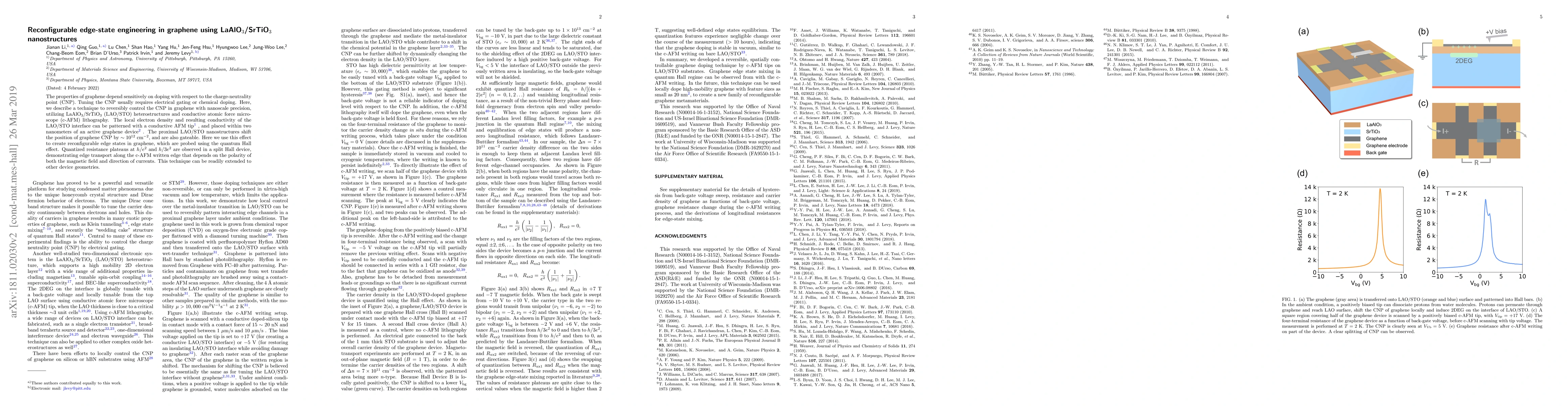
The properties of graphene depend sensitively on doping with respect to the charge-neutrality point (CNP). Tuning the CNP usually requires electrical gating or chemical doping. Here, we describe a technique to reversibly control the CNP in graphene with nanoscale precision, utilizing LaAlO$_3$/SrTiO$_3$ (LAO/STO) heterostructures and conductive atomic force microscope (c-AFM) lithography. The local electron density and resulting conductivity of the LAO/STO interface can be patterned with a conductive AFM tip, and placed within two nanometers of an active graphene device. The proximal LAO/STO nanostructures shift the position of graphene CNP by ~ $10^{12}$ cm$^{-2}$, and are also gateable. Here we use this effect to create reconfigurable edge states in graphene, which are probed using the quantum Hall effect. Quantized resistance plateaus at $h/e^2$ and $h/3e^2$ are observed in a split Hall device, demonstrating edge transport along the c-AFM written edge that depends on the polarity of both the magnetic field and direction of currents. This technique can be readily extended to other device geometries.
Generated Sep 04, 2025
The research used LaAlO$_3$/SrTiO$_3$ nanostructures and conductive atomic force microscope (c-AFM) lithography to reversibly control the charge-neutrality point in graphene.
This research demonstrates a new method for controlling the charge-neutrality point in graphene, which could have important implications for the development of next-generation electronic devices.
The development of a new method for controlling the charge-neutrality point in graphene using LaAlO$_3$/SrTiO$_3$ nanostructures and conductive atomic force microscope (c-AFM) lithography.
This research demonstrates a novel approach to controlling the charge-neutrality point in graphene, which could have important implications for the development of next-generation electronic devices.
Current paper (gray), citations (green), references (blue)
Display is limited for performance on very large graphs.
Title | Authors | Year | Actions |
---|
Comments (0)