This research presents a reconfigurable FeFET-based TD-nvIMC accelerator with integrated CAM, DE chain, and TDC, fabricated in 28 nm CPOM. It supports binary MAC operations using XOR/AND for multiplication and Boolean logic, demonstrating a FeFET-based nvIMC with 550 ps step size.
Reconfigurable Time-Domain In-Memory Computing Marco using CAM FeFET with Multilevel Delay Calibration in 28 nm CMOS
Publication
Metrics
AI Quick Summary
This paper presents a reconfigurable time-domain nonvolatile in-memory computing accelerator using a ferroelectric FET content-addressable memory array, achieving a 2000× improvement over previous works. The architecture compensates for delay element mismatch with multilevel state calibration, enabling high throughput and energy efficiency.
Quick Answers
What methodology did the authors use?
This research presents a reconfigurable FeFET-based TD-nvIMC accelerator with integrated CAM, DE chain, and TDC, fabricated in 28 nm CPOM. It supports binary MAC operations using XOR/AND for multiplication and Boolean logic, demonstrating a FeFET-based nvIMC with 550 ps step size. More in Methodology →
What are the key results?
Achieved 550 ps delay step size, an improvement of ~2000× from previous works. — Demonstrated write-disturb prevention and multilevel state (MLS) using isolated bulks. More in Key Results →
Why is this work significant?
This work is significant as it presents a high-performance, energy-efficient TD-nvIMC architecture suitable for advanced in-memory computing applications, addressing limitations of analog-based nvIMCs by using time-domain techniques. More in Significance →
What are the main limitations?
The proof-of-concept (PoC) area is relatively small (17.6×30.7 µm2). — Further research is needed to scale the architecture to larger arrays for practical applications. More in Limitations →
Abstract
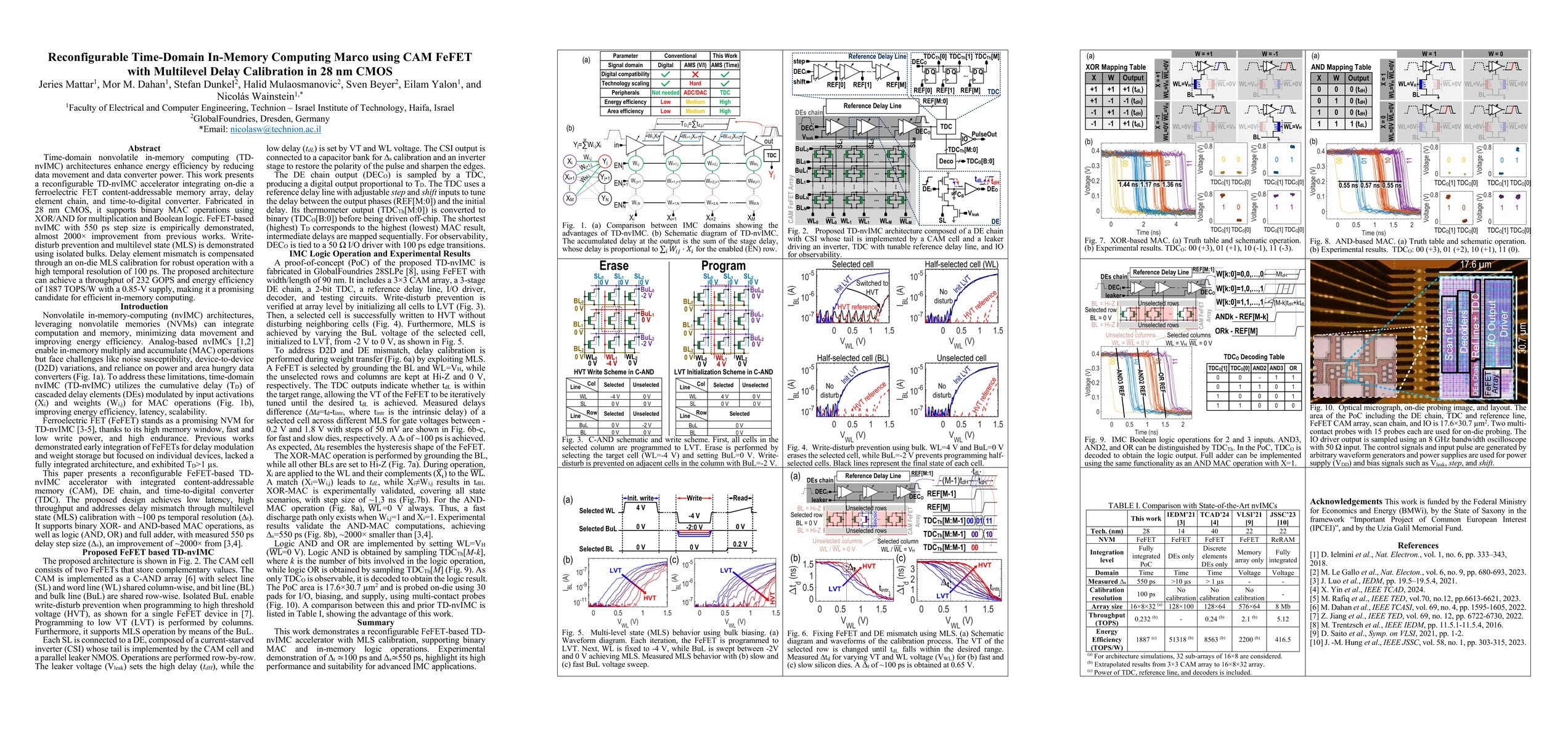
Time-domain nonvolatile in-memory computing (TD-nvIMC) architectures enhance energy efficiency by reducing data movement and data converter power. This work presents a reconfigurable TD-nvIMC accelerator integrating on-die a ferroelectric FET content-addressable memory array, delay element chain, and time-to-digital converter. Fabricated in 28 nm CMOS, it supports binary MAC operations using XOR/AND for multiplication and Boolean logic. FeFET-based nvIMC with 550 ps step size is empirically demonstrated, almost 2000$\times$ improvement from previous works. Write-disturb prevention and multilevel state (MLS) is demonstrated using isolated bulks. Delay element mismatch is compensated through an on-die MLS calibration for robust operation with a high temporal resolution of 100 ps. The proposed architecture can achieve a throughput of 232 GOPS and energy efficiency of 1887 TOPS/W with a 0.85-V supply, making it a promising candidate for efficient in-memory computing.
Key Findings, in focus
Seven facets of this paper, analysed and brought into focus by AI.
This work is significant as it presents a high-performance, energy-efficient TD-nvIMC architecture suitable for advanced in-memory computing applications, addressing limitations of analog-based nvIMCs by using time-domain techniques.
- Achieved 550 ps delay step size, an improvement of ~2000× from previous works.
- Demonstrated write-disturb prevention and multilevel state (MLS) using isolated bulks.
- Compensated delay element mismatch through on-die MLS calibration, achieving a high temporal resolution of 100 ps.
- Demonstrated throughput of 232 GOPS and energy efficiency of 1887 TOPS/W with a 0.85-V supply.
- Supported binary XOR- and AND-based MAC operations, as well as logic (AND, OR) and full adder.
This work is significant as it presents a high-performance, energy-efficient TD-nvIMC architecture suitable for advanced in-memory computing applications, addressing limitations of analog-based nvIMCs by using time-domain techniques.
This paper introduces a reconfigurable FeFET-based TD-nvIMC accelerator with integrated CAM, DE chain, and TDC, demonstrating a high-performance, energy-efficient architecture for in-memory computing.
The proposed architecture combines FeFET-based nvIMC with time-domain techniques, achieving significant improvements in delay step size and temporal resolution compared to previous works, while also addressing limitations of analog-based nvIMCs.
- The proof-of-concept (PoC) area is relatively small (17.6×30.7 µm2).
- Further research is needed to scale the architecture to larger arrays for practical applications.
- Explore scaling the architecture to larger arrays for practical use cases.
- Investigate the integration of this TD-nvIMC accelerator with other system components for end-to-end applications.
Authors
PDF Preview
Related Papers
No references found for this paper.
Discussion 0