Reduced Material Loss in Thin-film Lithium Niobate Waveguides

Source: ArXiv

AI Quick Summary

This paper investigates the material limitations of thin-film lithium niobate waveguides, demonstrating that they can achieve an exceptionally high quality factor of $Q\approx 1.8\times10^{8}$, corresponding to a propagation loss of only 0.2 dB/m, significantly reducing material loss for advanced optical applications.

Share: Share on X LinkedIn

Summary

Thin-film lithium niobate has shown promise for scalable applications ranging from single-photon sources to high-bandwidth data communication systems. Realization of the next generation high-performance classical and quantum devices, however, requires much lower optical losses than the current state of the art ($\sim$10 million). Unfortunately, material limitations of ion-sliced thin-film lithium niobate have not been explored, and therefore it is unclear how high-quality factor can be achieved in this platform. Here we evaluate the material limited quality factor of thin-film lithium niobate photonic platform can be as high as $Q\approx 1.8\times10^{8}$ at telecommunication wavelengths, corresponding to a propagation loss of 0.2 dB/m.

AI Key Findings

Generated Sep 02, 2025

Methodology

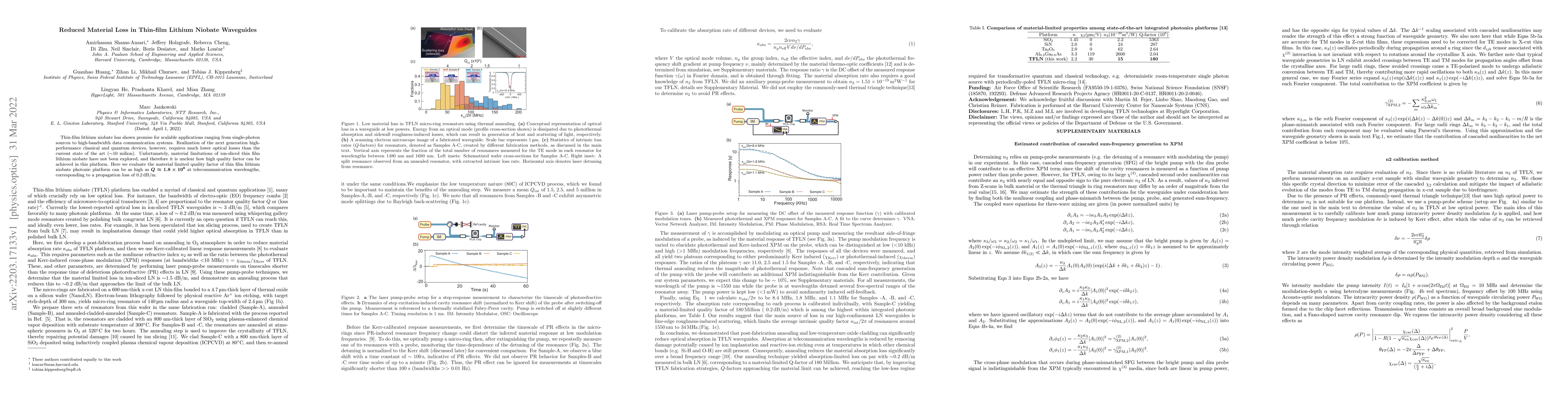
The research methodology involved calibrating the absorption rate of different thin-film lithium niobate (TFLN) devices using a laser pump-probe setup to measure the DCoffset (γ) of the material response in the Fourier domain. The material absorption rate was calculated using Eq. (1), requiring knowledge of n2 from TFLN, which was obtained through an auxiliary pump-probe measurement (n2 = 1.51 × 10^-19 m²/W). The study distinguished photothermal and Kerr-induced cross-phase modulation (XPM) responses at low (<10 kHz) and high (>1 MHz) modulation frequencies, respectively.

Key Results

  • The material-limited quality factor of TFLN photonic platform was found to be as high as Q ≈ 1.8 × 10^8 at telecommunication wavelengths, corresponding to a propagation loss of 0.2 dB/m.
  • Sample C yielded a material-limited absorption rate, reducing material absorption loss significantly over a broad frequency range, with an absorption-limited loss on par with ~0.2 dB/m measured in bulk LN, corresponding to a material-limited Q-factor of 180 million.
  • The main source of loss in high-confinement LN waveguides was identified as line-edge roughness-induced scattering, limiting the average intrinsic quality factor κint/2π of resonances around 1550 nm to 34 MHz.
  • Post-fabrication annealing and low-temperature oxide cladding significantly reduced optical absorption in TFLN waveguides, bringing the loss down to values comparable to those in bulk LN.

Significance

This research is significant as it demonstrates the potential of TFLN waveguides for next-generation high-performance classical and quantum devices by achieving much lower optical losses than the current state of the art (~10 million). The findings suggest that with improved fabrication strategies, Q-factors approaching the material limit can be achieved, reaching the low-loss regime required for transformative quantum and classical technologies.

Technical Contribution

The paper presents a novel approach to reducing material absorption losses in thin-film lithium niobate waveguides through post-fabrication annealing and low-temperature oxide cladding, achieving a material-limited Q-factor of 180 million at telecommunication wavelengths.

Novelty

This work distinguishes itself by focusing on material limitations and ion-sliced thin-film lithium niobate, providing a comprehensive evaluation of its potential for high-performance photonic devices. The findings offer a pathway to overcome current limitations in TFLN platforms and pave the way for next-generation low-loss integrated photonic systems.

Limitations

  • The study was conducted on thin-film lithium niobate, and the results might not directly translate to other photonic platforms.
  • The research focused on specific waveguide geometries and material properties; further investigation is needed to generalize the findings for a broader range of integrated photonic platforms.

Future Work

  • Investigate the scalability of annealing techniques to other TFLN fabrication processes and waveguide geometries.
  • Explore the impact of varying TFLN material properties, such as crystal orientation and doping, on optical performance.

Paper Details

PDF Preview

Download PDF

Key Terms

lithium (0.356)
film (0.288)
platform (0.231)
material (0.194)
quality (0.173)
factor (0.165)
high (0.159)
db (0.157)

Citation Network

Current paper (gray), citations (green), references (blue)

Display is limited for performance on very large graphs.

Current Paper
Citations
References
Click to view
Title Authors Year Actions

Comments (0)

This website uses cookies to ensure you get the best experience. Learn more