AI Quick Summary
This paper presents a reliable optical method for identifying the layer number of Au-assisted exfoliated MoS$_2$ and WS$_2$ films using reflection spectroscopic fingerprints. The method leverages the intensity of reflection peaks in white light spectra to accurately determine layer numbers across a broad thickness range.
Paper Preview
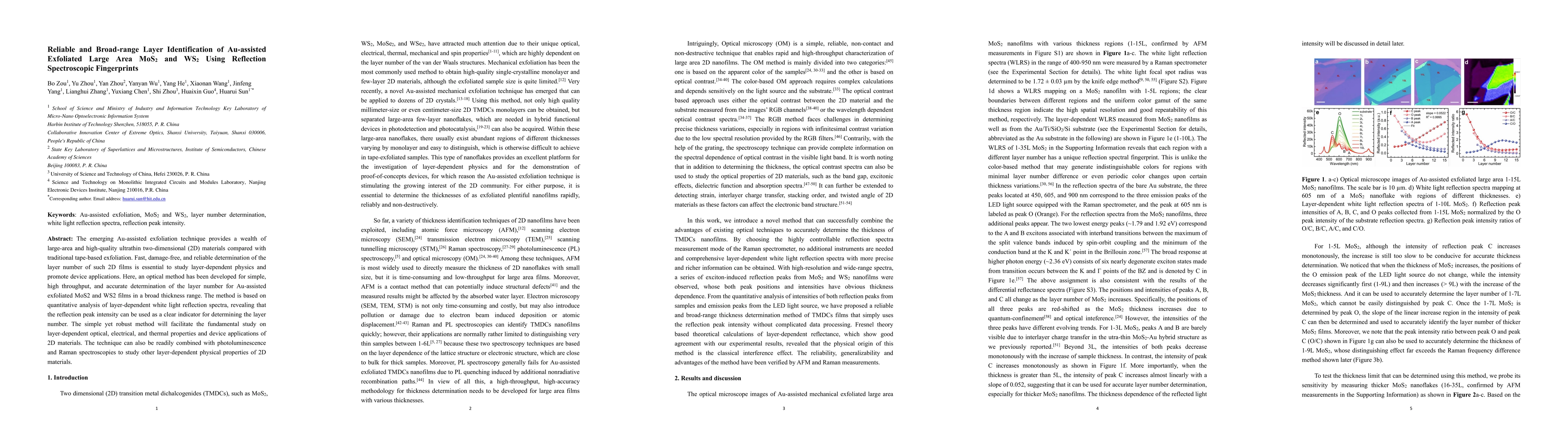
Abstract
The emerging Au-assisted exfoliation technique provides a wealth of large-area and high-quality ultrathin two-dimensional (2D) materials compared with traditional tape-based exfoliation. Fast, damage-free, and reliable determination of the layer number of such 2D films is essential to study layer-dependent physics and promote device applications. Here, an optical method has been developed for simple, high throughput, and accurate determination of the layer number for Au-assisted exfoliated MoS$_2$ and WS$_2$ films in a broad thickness range. The method is based on quantitative analysis of layer-dependent white light reflection spectra, revealing that the reflection peak intensity can be used as a clear indicator for determining the layer number. The simple yet robust method will facilitate the fundamental study on layer-dependent optical, electrical, and thermal properties and device applications of 2D materials. The technique can also be readily combined with photoluminescence and Raman spectroscopies to study other layer-dependent physical properties of 2D materials.
AI Key Findings
Get AI-generated insights about this paper's methodology, results, and significance.
Paper Details
PDF Preview
Key Terms
Citation Network
Current paper (gray), citations (green), references (blue)
Display is limited for performance on very large graphs.
Similar Papers
Found 4 papersTwist angle dependent electronic properties of exfoliated single layer MoS$_2$ on Au(111)
Ishita Pushkarna, Árpád Pásztor, Christoph Renner
| Title | Authors | Year | Actions |
|---|
Comments (0)