ArxivLens

Quick Summary:

This paper investigates resistive switching in Cu/MgO/MoS2/Cu devices fabricated using magnetron sputtering, finding that inserting a MoS2 layer significantly improves the switching ratio and reduces reset voltage. The MoS2 layer regulates the interface barrier, enhancing device performance, with the Cu/MgO/MoS2/Cu configuration showing the best results for practical applications.

DOI: 10.7498/aps.74.20241298
arXiv Id: 2504.02384
Comments: The paper contains 13 pages and 8 figures
Date Published: 2025-04-03
Date Updated: 2025-04-03

Key Terms (TF-IDF):

No key terms available for this paper.

Summary:

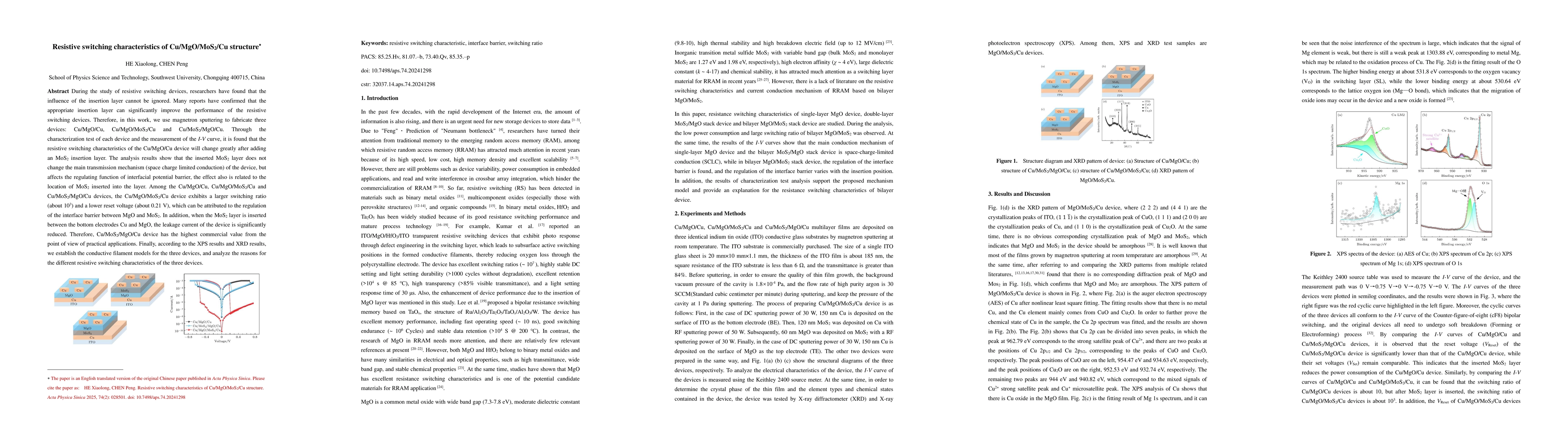
During the study of resistive switching devices, researchers have found that the influence of the insertion layer cannot be ignored. Many reports have confirmed that the appropriate insertion layer can significantly improve the performance of the resistive switching devices. Therefore, in this work, we use magnetron sputtering to fabricate three devices: Cu/MgO/Cu, Cu/MgO/MoS2/Cu and Cu/MoS2/MgO/Cu. Through the characterization test of each device and the measurement of the I-V curve, it is found that the resistive switching characteristics of the Cu/MgO/Cu device will change greatly after adding an MoS2 insertion layer. The analysis results show that the inserted MoS2 layer does not change the main transmission mechanism (space charge limited conduction) of the device, but affects the regulating function of interfacial potential barrier, the effect also is related to the location of MoS2 inserted into the layer. Among the Cu/MgO/Cu, Cu/MgO/MoS2/Cu and Cu/MoS2/MgO/Cu devices, the Cu/MgO/MoS2/Cu device exhibits a larger switching ratio (about 103) and a lower reset voltage (about 0.21 V), which can be attributed to the regulation of the interface barrier between MgO and MoS2. In addition, when the MoS2 layer is inserted between the bottom electrodes Cu and MgO, the leakage current of the device is significantly reduced. Therefore, Cu/MoS2/MgO/Cu device has the highest commercial value from the point of view of practical applications. Finally, according to the XPS results and XRD results, we establish the conductive filament models for the three devices, and analyze the reasons for the different resistive switching characteristics of the three devices.

Citation & Reference Network Visualization

This graph shows how this paper is connected to other research. The current paper is shown in dark gray, papers that cite it are in green, and papers it references are in blue. You can:

Current Paper
Papers citing this work (Citations)
Papers cited by this work (References)

• Hover over any node to see the paper title

• Click a node to view that paper's details

• Drag nodes to rearrange the graph

• Use the zoom controls (bottom right) to zoom in/out

Citations and References

No citations found for this paper.

Similar Papers

Cu Intercalation-stabilized 1T'-MoS2 with Electrical Insulating Behavior

Yunhao Zhang, Yue Gu, Qiang Wei, Jingwei Wang, Yujie Sun, Xiaolong Zou, Junyang Tan, Huiyu Nong, Qinke Wu, Bilu Liu, Rongjie Zhang

Published: 2025-02-01

Unusual flat and extended morphology of intercalated Cu under MoS2

Zhe Fei, Yong Han, Dapeng Jing, Marek Kolmer, Michael C. Tringides, James W. Evans

Published: 2022-09-23

Comments (0)

This website uses cookies to ensure you get the best experience. Learn more