Resistivity size effect due to surface steps on ruthenium thin films computed with a realistic tight-binding model
Publication
Metrics
AI Quick Summary
Researchers used a tight-binding model to study how surface steps affect the resistivity of ruthenium thin films, finding that even with steps, the effect is smaller than previously thought, making Ru a promising material for interconnects.
Paper Preview
Abstract
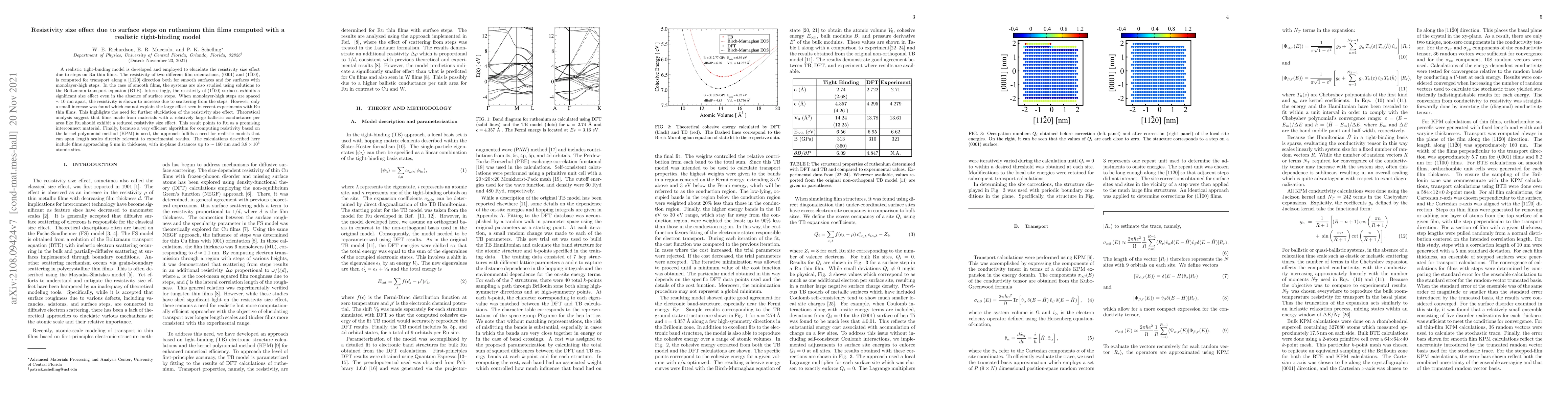
A realistic tight-binding model is developed and employed to elucidate the resistivity size effect due to steps on Ru thin films. The resistivity of two different film orientations, $(0001)$ and $(1 \bar{1}00)$, is computed for transport along a $[1 1 \bar{2} 0]$ direction both for smooth surfaces and for surfaces with monolayer-high steps. In the case of smooth films, the systems are also studied using solutions to the Boltzmann transport equation (BTE). Interestingly, the resistivity of $(1 \bar{1}00)$ surfaces exhibits a significant size effect even in the absence of surface steps. When monolayer-high steps are spaced $\sim 10$ nm apart, the resistivity is shown to increase due to scattering from the steps. However, only a small increase was found which cannot explain the large effect seen in recent experiments with Ru thin films. This highlights the need for further elucidation of the resistivity size effect. Theoretical analysis suggest that films made from materials with a relatively large ballistic conductance per area like Ru should exhibit a reduced resistivity size effect. This result points to Ru as a promising interconnect material. Finally, because a very efficient algorithm for computing resistivity based on the kernel polynomial method (KPM) is used, the approach fulfills a need for realistic models that can span length scales directly relevant to experimental results. The calculations described here include films approaching $5$ nm in thickness, with in-plane distances up to $\sim 160$ nm and $3.8\times10^{5}$ atomic sites.
AI Key Findings
Get AI-generated insights about this paper's methodology, results, significance, and more — seven facets brought into focus.
Impact
Paper Details
Authors
PDF Preview
Key Terms
Citation Network
Current paper (gray), citations (green), references (blue)
Display is limited for performance on very large graphs.
Discussion 0