Resolving the positions of defects in superconducting quantum bits

PDF

Publication

Published: Mar 12, 2020
Categories: quant-ph, cond-mat.mes-hall, physics.ins-det

Metrics

Source: ArXiv

Quick Actions

View PDF

AI Quick Summary

Researchers develop a technique to locate defects in superconducting quantum bits using electric fields and simulations, offering a tool for improving material quality and nano-fabrication procedures.

Quick Answers

What is "Resolving the positions of defects in superconducting quantum bits" about?

Researchers develop a technique to locate defects in superconducting quantum bits using electric fields and simulations, offering a tool for improving material quality and nano-fabrication procedures.

What methodology did the authors use?

The research employed a combination of theoretical modeling and experimental techniques to investigate two-level systems in superconducting transmon qubits. More in Methodology →

What are the key results?

Observation of quantum oscillations between the qubit and a microresonator — Detection of surface participation and dielectric loss in superconducting qubits More in Key Results →

Why is this work significant?

This research sheds light on the behavior of two-level systems in superconducting transmon qubits, with potential implications for quantum computing and information processing. More in Significance →

What are the main limitations?

Limited sample size due to experimental constraints — Potential biases introduced by measurement techniques More in Limitations →

Paper Preview

Abstract

Solid-state quantum coherent devices are quickly progressing. Superconducting circuits, for instance, have already been used to demonstrate prototype quantum processors comprising a few tens of quantum bits. This development also revealed that a major part of decoherence and energy loss in such devices originates from a bath of parasitic material defects. However, neither the microscopic structure of defects nor the mechanisms by which they emerge during sample fabrication are understood. Here, we present a technique to obtain information on locations of defects relative to the thin film edge of the qubit circuit. Resonance frequencies of defects are tuned by exposing the qubit sample to electric fields generated by electrodes surrounding the chip. By determining the defect's coupling strength to each electrode and comparing it to a simulation of the field distribution, we obtain the probability at which location and at which interface the defect resides. This method is applicable to already existing samples of various qubit types, without further on-chip design changes. It provides a valuable tool for improving the material quality and nano-fabrication procedures towards more coherent quantum circuits.
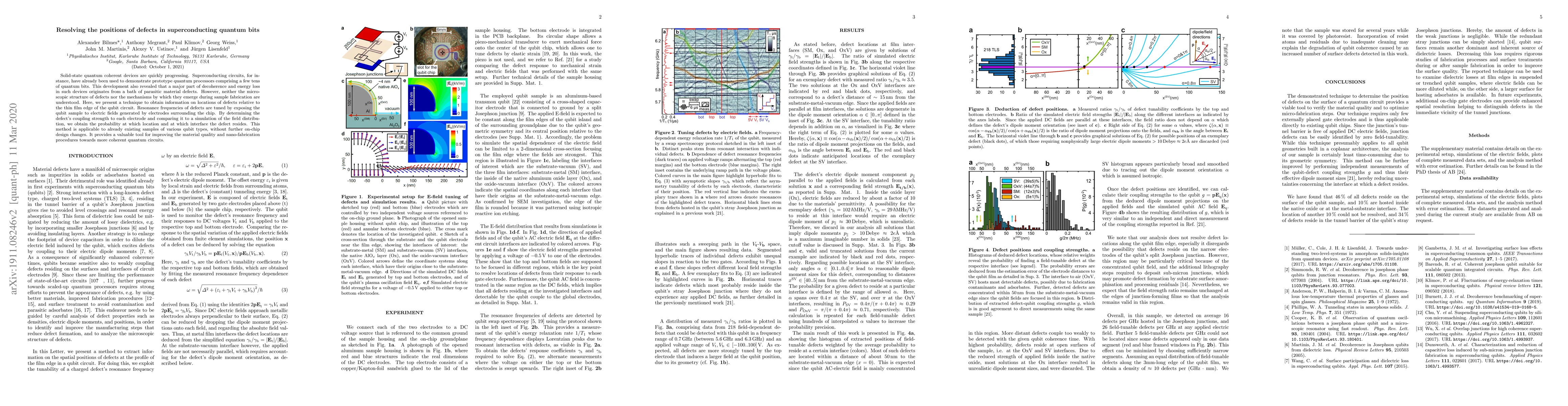
AI Key Findings

Generated Sep 04, 2025

Methodology — What approach did the authors take?

The research employed a combination of theoretical modeling and experimental techniques to investigate two-level systems in superconducting transmon qubits.

Key Results — What are the main findings?

  • Observation of quantum oscillations between the qubit and a microresonator
  • Detection of surface participation and dielectric loss in superconducting qubits
  • Investigation of strain-tuning effects on individual atomic tunneling systems

Significance — Why does this research matter?

This research sheds light on the behavior of two-level systems in superconducting transmon qubits, with potential implications for quantum computing and information processing.

Technical Contribution — What is the technical contribution?

The development and implementation of a novel measurement technique to detect quantum oscillations between the qubit and microresonator.

Novelty — What is new about this work?

This work presents new insights into the behavior of two-level systems in superconducting transmon qubits, with potential applications in quantum computing and information processing.

Limitations — What are the limitations of this study?

  • Limited sample size due to experimental constraints
  • Potential biases introduced by measurement techniques

Future Work — What did the authors propose for future work?

  • Investigation of surface participation effects on qubit coherence times
  • Development of new experimental techniques to probe two-level systems
  • Theoretical modeling of strain-tuning effects on atomic tunneling systems

Paper Details

Paper ID: 1911.08246
License: http://creativecommons.org/licenses/by-nc-sa/4.0/
Categories:
quant-ph cond-mat.mes-hall physics.ins-det

How to Cite This Paper

BibTeX
@article{bilmes2020resolving,
  title         = {Resolving the positions of defects in superconducting quantum bits},
  author        = {Bilmes, Alexander and Ustinov, Alexey V. and Megrant, Anthony and others},
  year          = {2020},
  eprint        = {1911.08246},
  archivePrefix = {arXiv},
  primaryClass  = {quant-ph},
  doi           = {10.1038/s41598-020-59749-y},
}
APA 7
Bilmes, A., Ustinov, A., Megrant, A., Weiss, G., Martinis, J., Lisenfeld, J., & Klimov, P. (2020). Resolving the positions of defects in superconducting quantum bits. arXiv. https://doi.org/10.1038/s41598-020-59749-y
MLA 9
Bilmes, Alexander, et al. "Resolving the positions of defects in superconducting quantum bits." arXiv, 2020, doi.org/10.1038/s41598-020-59749-y.

Key Terms

defects (0.271)
qubit (0.230)
chip (0.221)
fabrication (0.212)
circuits (0.212)
defect (0.205)
coherent (0.166)
material (0.158)

Citation Network

Current paper (gray), citations (green), references (blue)

Display is limited for performance on very large graphs.

Current Paper
Citations
References
Click to view
Title Authors Year Actions

Comments (0)

This website uses cookies to ensure you get the best experience. Learn more