Reviving holographic photonic integration

Source: ArXiv

AI Quick Summary

This paper addresses the challenges in integrating thick holograms within waveguiding structures for photonics, focusing on the difficulty of achieving high fabrication accuracy and the complexity of numerical design for large optical neural networks. It highlights the need for overcoming large refractive index differences in silicon photonics.

Share: Share on X LinkedIn

Summary

Photonic integration of thick holograms in waveguiding structures could be considered the chimera of photonics; multi-faceted and hard to tame. It is the fundamental, and hence indispensable, concept behind compact and monolithically integrated linear optical transformation1. The true relevance of this becomes apparent in the high-dimensional context of unconventional optical computing, that is, in optical neural networks. Yet, integrating such holographic connections is very challenging. It demands high fabrication accuracy, and numerical design of the circuit is often non-tractable for large architectures. Both challenges are intrinsically linked to the usually large refractive index differences between sections of such holographic optical waveguides when using standard techniques of silicon photonics.
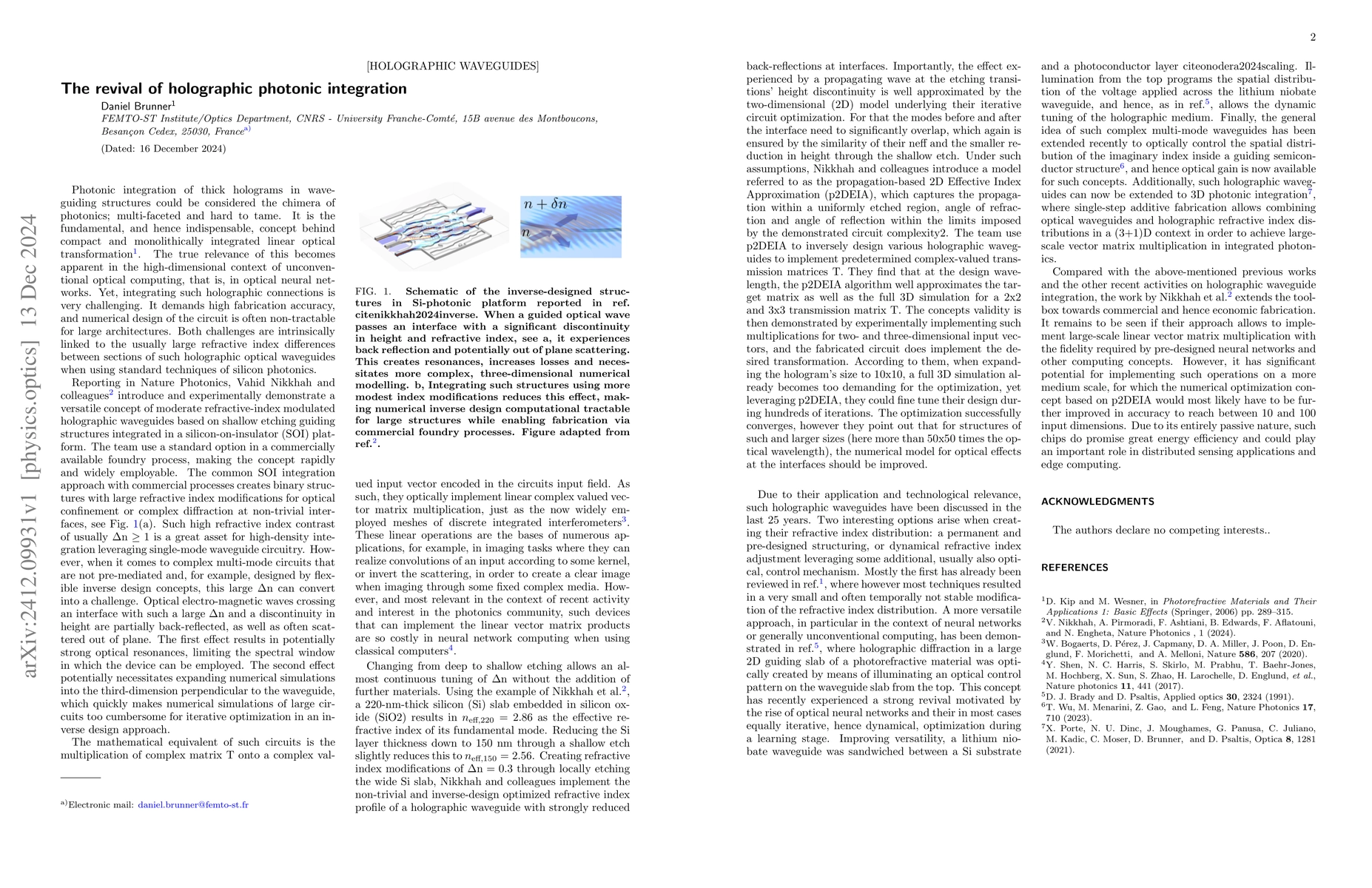
AI Key Findings

Generated Sep 03, 2025

Methodology

The research introduces a concept of moderate refractive-index modulated holographic waveguides based on shallow etching guiding structures integrated in a silicon-on-insulator (SOI) platform, utilizing a standard option in a commercially available foundry process.

Key Results

  • Introduction of a versatile concept for holographic waveguides with reduced refractive index differences, making numerical design of large architectures more tractable.
  • Demonstration of inverse-designed structures that implement linear complex-valued vector matrix multiplication, similar to widely employed mesh interferometers.
  • Validation of the propagation-based 2D Effective Index Approximation (p2DEIA) algorithm, which approximates target matrices well for 2x2 and 3x3 transmission matrices.

Significance

This work is significant as it extends the toolbox towards commercial and economic fabrication of holographic waveguides, potentially impacting large-scale linear vector matrix multiplication in integrated photonics, particularly for neural networks and unconventional computing.

Technical Contribution

The main technical contribution is the introduction of a novel approach for designing holographic waveguides with reduced refractive index contrast, enabling more tractable numerical design for large architectures.

Novelty

This research stands out by presenting a commercially viable method for creating holographic waveguides with moderate refractive index modulations, which simplifies numerical design and fabrication for large-scale integrated photonic systems.

Limitations

  • The p2DEIA model may need improvement for numerical modeling of optical effects at interfaces for structures larger than 50x50 optical wavelengths.
  • The approach's potential for implementing large-scale linear vector matrix multiplication with the required fidelity for pre-designed neural networks remains to be seen.

Future Work

  • Further improvement of numerical optimization concepts based on p2DEIA for increased accuracy in handling 10 to 100 input dimensions.
  • Exploration of entirely passive chips for great energy efficiency in distributed sensing applications and edge computing.

Paper Details

PDF Preview

Download PDF

Citation Network

Current paper (gray), citations (green), references (blue)

Display is limited for performance on very large graphs.

Current Paper
Citations
References
Click to view

No citations found for this paper.

Comments (0)

This website uses cookies to ensure you get the best experience. Learn more