Publication
Metrics
AI Quick Summary
This paper reports the first observation of significant ballistic electron transport at room temperature in InSb quantum well nanodevices, evidenced by a negative bend resistance signature. Effective growth and processing strategies enable practical exploitation of room temperature ballistic effects in InSb/AlInSb quantum wells.
Paper Preview
Abstract
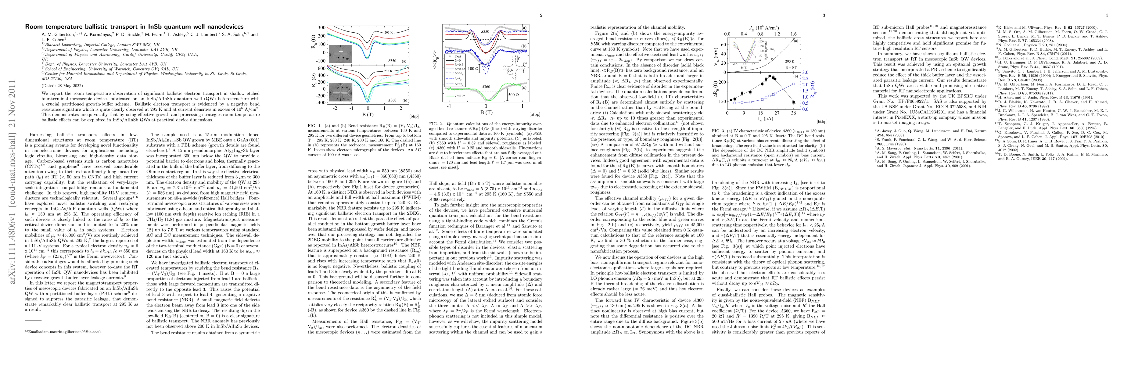
We report the room temperature observation of significant ballistic electron transport in shallow etched four-terminal mesoscopic devices fabricated on an InSb/AlInSb quantum well (QW) heterostructure with a crucial partitioned growth-buffer scheme. Ballistic electron transport is evidenced by a negative bend resistance signature which is quite clearly observed at 295 K and at current densities in excess of 10$^{6}$ A/cm$^{2}$. This demonstrates unequivocally that by using effective growth and processing strategies, room temperature ballistic effects can be exploited in InSb/AlInSb QWs at practical device dimensions.
AI Key Findings
Get AI-generated insights about this paper's methodology, results, significance, and more — seven facets brought into focus.
Impact
Paper Details
PDF Preview
Key Terms
Citation Network
Current paper (gray), citations (green), references (blue)
Display is limited for performance on very large graphs.
Discussion 0