01
MethodologyHow they did it
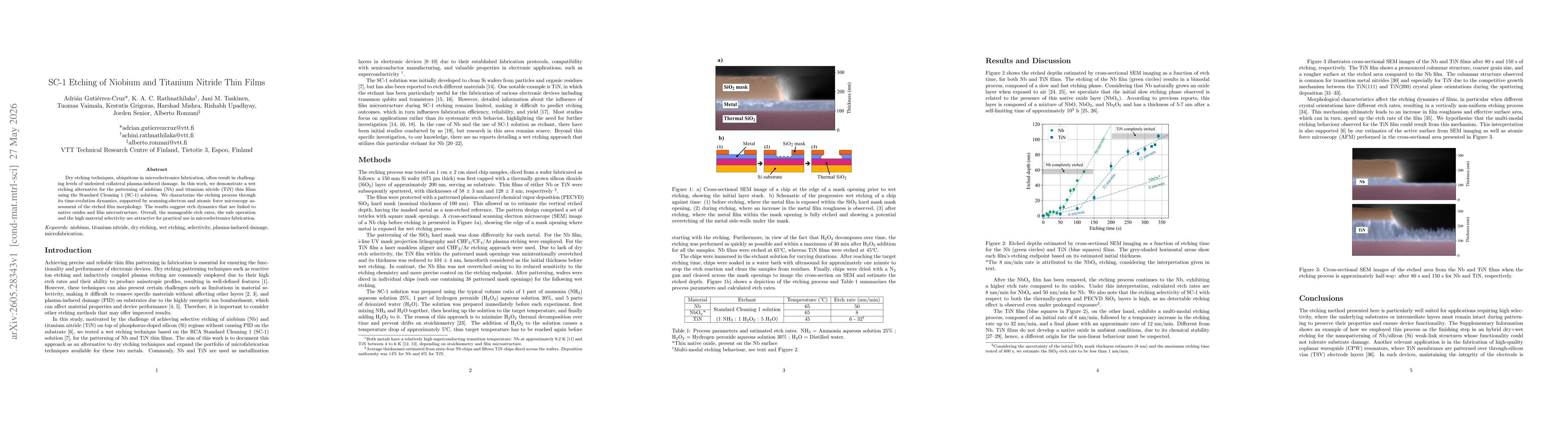
The study employed SC-1 wet etching on Nb and TiN thin films patterned with SiO2 hard masks. Nb and TiN films (58±3 nm Nb, 128±3 nm TiN) were deposited on Si/SiO2 substrates and patterned using lithography, followed by SC-1 etching at a controlled temperature with a defined NH3:H2O2:H2O composition. Etch progress was monitored via time-evolution experiments, and post-etch characterization included SEM and AFM to assess morphology, with special attention to oxide-related and microstructural effects on etch dynamics.
Discussion 0