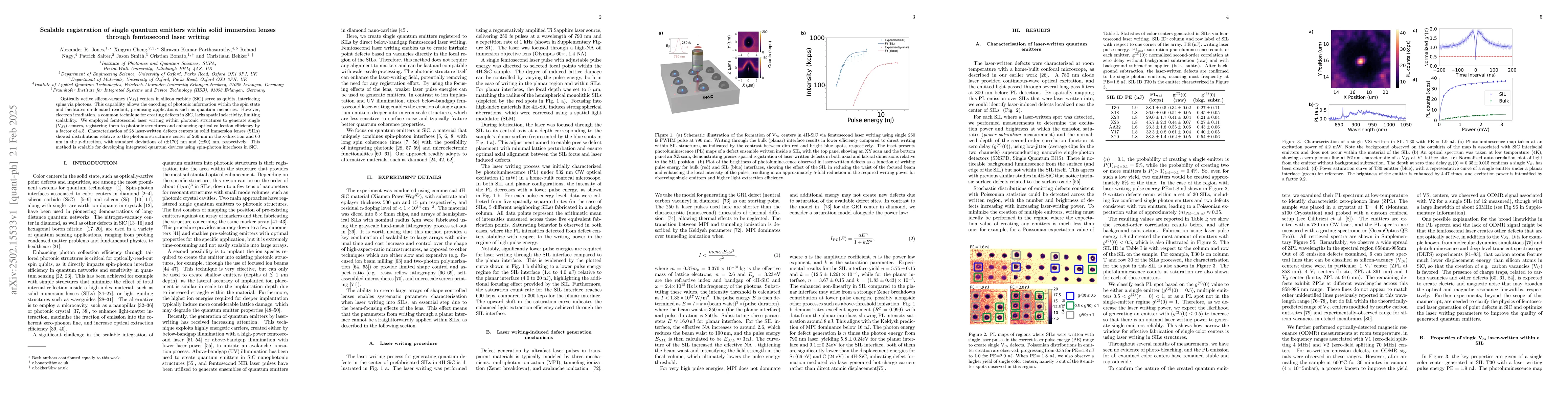
Optically active silicon-vacancy (V$_{Si}$) centers in silicon carbide (SiC)
serve as qubits, interfacing spins via photons. This capability allows the
encoding of photonic information within the spin state and facilitates
on-demand readout, promising applications such as quantum memories. However,
electron irradiation, a common technique for creating defects in SiC, lacks
spatial selectivity, limiting scalability. We employed femtosecond laser
writing within photonic structures to generate single (V$_{Si}$) centers,
registering them to photonic structures and enhancing optical collection
efficiency by a factor of 4.5. Characterization of 28 laser-written defects
centers in solid immersion lenses (SILs) showed distributions relative to the
photonic structure's center of 260 nm in the x-direction and 60 nm in the
y-direction, with standard deviations of $\pm 170$ nm and $\pm 90$ nm,
respectively. This method is scalable for developing integrated quantum devices
using spin-photon interfaces in SiC.
Discussion 0