The research introduces a highly scalable, universal, and conformal direct electrodes microprinting technique using PPC/PVA copolymer for transferring wafer-scale, micropatterned electrodes onto diverse substrates, including complex geometries.
Publication
Metrics
AI Quick Summary
This paper introduces a scalable, conformal microprinting technique using PPC/PVA copolymer for high-performance van der Waals-integrated 2D electronics. The method enables wafer-scale micropatterned electrode transfer onto various substrates, achieving record-high carrier mobility in WSe2 devices and outstanding mechanical robustness in flexible MoS2 transistors.
Quick Answers
What is "Scalable, universal and conformal direct electrodes microprinting for high-performance van der Waals-integrated two-dimensional electronics and flexible applications" about?
This paper introduces a scalable, conformal microprinting technique using PPC/PVA copolymer for high-performance van der Waals-integrated 2D electronics. The method enables wafer-scale micropatterned electrode transfer onto various substrates, achieving record-high carrier mobility in WSe2 devices and outstanding mechanical robustness in flexible MoS2 transistors.
What methodology did the authors use?
The research introduces a highly scalable, universal, and conformal direct electrodes microprinting technique using PPC/PVA copolymer for transferring wafer-scale, micropatterned electrodes onto diverse substrates, including complex geometries. More in Methodology →
What are the key results?
Achieved near-ideal ohmic contacts with low contact resistance in 2D field-effect transistors (FETs) using few-layer TMDC flakes. — Demonstrated a record-high carrier mobility of up to 334 cm² V⁻¹ s⁻¹ for a WSe₂ device. More in Key Results →
Why is this work significant?
This work represents a significant advance in the fabrication of flexible 2D electronics, paving the way for numerous emerging technologies by enabling high-performance, large-scale, and flexible 2D electronics across diverse substrates. More in Significance →
What are the main limitations?
The study did not compare the microprinting technique with other existing transfer methods in terms of cost and scalability for industrial applications. — The long-term stability and reliability of the microprinted electrodes under various environmental conditions were not extensively explored. More in Limitations →
Abstract
Two-dimensional (2D) materials with extraordinary electrical properties, hold promising for large-scale, flexible electronics. However, their device performance could be hindered due to the excessive defects introduced via traditional electrode integration processes. Transfer printing techniques have been developed for van der Waals contacts integration, while existing techniques encounter limitations in achieving conformal electrode transfer and compatibility with flexible devices. Here we introduce a highly conformal microprinting technique utilizing polypropylene carbonate (PPC)/Polyvinyl alcohol (PVA) copolymer, which enables successful transfer of wafer-scale, micropatterned electrodes onto diverse substrates, including those with complex geometries. This technique, implemented with 2D transition metal dichalcogenides (TMDCs), yields 2D field-effect transistors with near-ideal ohmic contacts, and a record-high carrier mobility up to 334 cm2 V-1 s-1 for a WSe2 device. Furthermore, we fabricated transistor arrays on MoS2 thin film, which show uniform device performance. We also present the flexible MoS2 transistors that not only achieve a high electron mobility of up to 111 cm2 V-1 s-1 but also exhibit outstanding mechanical robustness. Our findings represent a significant leap forward in the fabrication of flexible 2D electronics, paving the way for numerous emerging technologies.
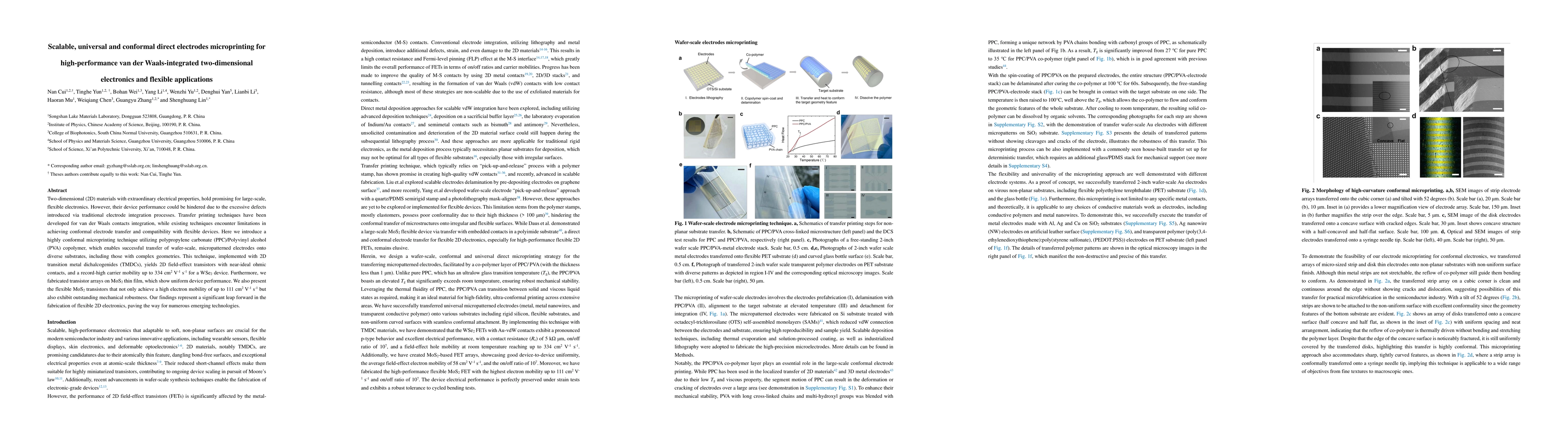
Key Findings, in focus
Seven facets of this paper, analysed and brought into focus by AI.
This work represents a significant advance in the fabrication of flexible 2D electronics, paving the way for numerous emerging technologies by enabling high-performance, large-scale, and flexible 2D electronics across diverse substrates.
- Achieved near-ideal ohmic contacts with low contact resistance in 2D field-effect transistors (FETs) using few-layer TMDC flakes.
- Demonstrated a record-high carrier mobility of up to 334 cm² V⁻¹ s⁻¹ for a WSe₂ device.
- Fabricated transistor arrays on MoS₂ thin film with uniform device performance.
- Produced flexible MoS₂ transistors with high electron mobility (up to 111 cm² V⁻¹ s⁻¹) and excellent mechanical robustness.
This work represents a significant advance in the fabrication of flexible 2D electronics, paving the way for numerous emerging technologies by enabling high-performance, large-scale, and flexible 2D electronics across diverse substrates.
The development of a highly conformal microprinting technique using PPC/PVA copolymer for successful transfer of wafer-scale, micropatterned electrodes onto diverse substrates, including complex geometries.
The microprinting technique overcomes limitations of existing transfer printing techniques by achieving conformal electrode transfer and compatibility with flexible devices, resulting in high-performance 2D electronics.
- The study did not compare the microprinting technique with other existing transfer methods in terms of cost and scalability for industrial applications.
- The long-term stability and reliability of the microprinted electrodes under various environmental conditions were not extensively explored.
- Investigate the cost-effectiveness and scalability of the microprinting technique for mass production.
- Explore the long-term stability and reliability of microprinted electrodes under different environmental conditions.
Impact
Paper Details
Authors
PDF Preview
Citation Network
Current paper (gray), citations (green), references (blue)
Display is limited for performance on very large graphs.
Discussion 0