Publication
Metrics
AI Quick Summary
This paper combines in-situ STM, AFM, and RHEED to study the scale-dependent optimized homoepitaxy of InAs(111)A, identifying two growth parameter regions for optimized surface roughness. It reveals a pure step-flow regime with minimal hillock formation and discusses the implications for future device engineering.
Paper Preview
Abstract
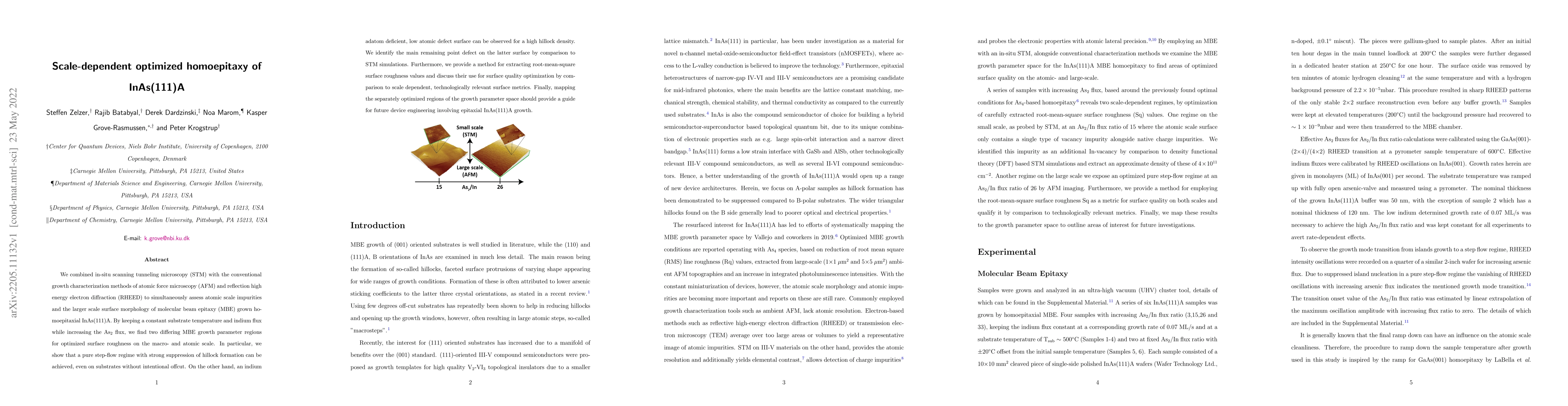
We combined in-situ scanning tunneling microscopy (STM) with the conventional growth characterization methods of atomic force microscopy (AFM) and reflection high energy electron diffraction (RHEED) to simultaneously assess atomic-scale impurities and the larger-scale surface morphology of molecular beam epitaxy (MBE) grown homoepitaxial InAs(111)A. By keeping a constant substrate temperature and indium flux while increasing the As$_2$ flux, we find two differing MBE growth parameter regions for optimized surface roughness on the macro and atomic scale. In particular, we show that a pure step-flow regime with strong suppression of hillock formation can be achieved, even on substrates without intentional offcut. On the other hand, an indium adatom deficient, low atomic defect surface can be observed for a high hillock density. We identify the main remaining point defect on the latter surface by comparison to STM simulations. Furthermore, we provide a method for extracting root-mean-square surface roughness values and discuss their use for surface quality optimization by comparison to scale-dependent, technologically relevant surface metrics. Finally, mapping the separately optimized regions of the growth parameter space should provide a guide for future device engineering involving epitaxial InAs(111)A growth.
AI Key Findings
Get AI-generated insights about this paper's methodology, results, significance, and more — seven facets brought into focus.
Impact
Paper Details
Authors
PDF Preview
Key Terms
Citation Network
Current paper (gray), citations (green), references (blue)
Display is limited for performance on very large graphs.
Discussion 0